


RTC – 4553AC
Page - 11
MQ - 342 - 01
(2) Control register 2
A3 A2 A1 A0
Name
D3 D2 D1 D0
Register
contents
1 1 1 0
CNT
2
BUSY
PONC
—
∗
Control register 2
Control register 2 provides flags for carry detect and power-on-clear detect.
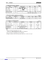
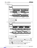
(a) BUSY bit (D3)
The BUSY bit serves for time/calendar counter digit carry detection.
BUSY bit
Mode
Meaning
0
Normal mode
Time/calendar counter read/write possible
1
Carry
Time/calendar counter read/write prohibited
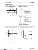
If the BUSY bit is "L", carry does not occur for at least 3.9 ms. (Also when read/write is carried out at point
"a" in the chart below, carry does not occur for 3.9 ms.)
Take the processing time into consideration and design the read/write operation to complete within 3.8 ms.
Clock read/write during carry
· Read It may not be possible to read correct data.
· Write Because the clock has priority, the write operation does not increment the counter.
(During carry, the result is the same as for a read operation.)
BUSY timing
Approx 0.5
µ
s
Carry pulse in IC
Read/write possible
Read/write prohibited (clock/calendar)
1 s
3.9 ms
“a”
BUSY bit
(b) PONC bit (D2)
The PONC bit is the power-on-clear detection bit (see next page). It is set to "1" when power-on-clear is
detected. The PONC bit is reset (1
→
0) by setting the SYSR bit to "1".
(c) D1 bit (bit marked "—")
When this bit is read, data are undefined.
(d) D0 bit (bit marked "
∗
")
When writing this bit, always set it to "0".
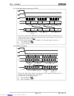
(3) Control register 3
Control registers 3 serves for reading and writing data for address mode switching and making system reset
settings.
The control register 3 applies to modes 0 - 2.
A3 A2 A1 A0
Name
D3 D2 D1 D0
Register
contents
1 1 1 1
CNT
3
SYSR
TEST
MS
1
MS
0
Control register 3
(a) SYSR bit (D3)
The SYSR bit serves for clearing all counter registers (see section on initialization on next page).
This bit is reset by making CS0 High and SCK Low.
(b) TEST bit (D2)
The TEST bit serves to switch the IC to the test mode.
Note Be sure to permanently set this bit to "0". Otherwise correct operation is not assured.
(c) MS1, MS0 bit (D1, D0)
The MS1 and MS0 bits serve for address switching.
MS1 MS0
Mode
name
Content
0
0
MODE 0
Time/calendar counters and control registers 1 - 3
0
1
MODE 0
Time/calendar counters and control registers 1 - 3
1
0
MODE 1
User RAM area (RA
0
- RA
59
) and control register 3
1
1
MODE 2
User RAM area (RA
60
- RA
119
) and control register 3
electronic components distributor


