background image

ST1 Series Product Manual, Rev. A

23

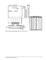
Figure 7. FX Model mechanical dimensions—top, side and end view

E

Breather Hole

Do not cover

FINGER GRIP

G

F

B

D

C

P

S

R

H

K

T

M

L

J

A

Inches

A
B
C
D
E
F

G
H

J

K

L

M

P
R
S
T

5.00

36.40
42.80

2x  25.78

29.25

7.61

10.00

1.60

2x    1.01

1.00

2x    1.00

1.65

23.00 
17.00 
10.51 

2X   3.30

0.197
1.433
1.685
1.015
1.152
0.299
0.394
0.063
0.040
0.039
0.039
0.065
0.906 
0.669 
0.414 
0.130

max   

± .006
± .004
± .003
± .010
± .010

min    

± .002
± .003
± .002
± .004
± .004
± .003 
± .020 
± .020 
± .004

max   

  ± .15  

± .10  

  ± .07  

 ± .25  

± .25  

min    

± .05  
± .07  
± .05  

min    

± .10  
± .07   
± .50   
± .50   
± .10  

Dimension Table

Millimeters

Summary of Contents for ST625211CF

Page 1: ...ST1 Series ST650211CF ST650211FX ST625211CF ST625211FX ...

Page 2: ......

Page 3: ...ST1 Series ST650211CF ST650211FX ST625211CF ST625211FX Rev A ...

Page 4: ...aFONE SeaBOARD SeaTDD and the Wave logo are either registered trade marks or trademarks of Seagate Technology LLC Other product names are registered trade marks or trademarks of their owners Seagate reserves the right to change without notice product offerings or specifications No part of this publication may be reproduced in any form without written permission of Seagate Technology LLC ...

Page 5: ...Revision status summary sheet Revision Date Sheets Affected Rev A 06 30 04 All ...

Page 6: ......

Page 7: ...Ambient temperature 12 2 10 2 Temperature gradient 12 2 10 3 Humidity 12 2 10 4 Altitude 12 2 10 5 Shock 13 2 10 6 Vibration 14 2 11 Acoustics 16 2 12 Electromagnetic immunity 16 2 13 Reliability 17 2 14 Agency certification 18 2 14 1 Safety certification 18 2 14 2 Electromagnetic compatibility 18 2 14 3 FCC verification 18 3 0 Configuring and mounting the drive 21 3 1 Handling and static discharg...

Page 8: ...vi ST1 Series Product Manual Rev A ...

Page 9: ...ace disc drive 1 Figure 3 Typical 3 3V startup and operation current profile 9 Figure 4 Location where tri axial accelerometer will be placed on S1 drive 13 Figure 5 Drive axis definition for S1 drives 13 Figure 6 CF model mechanical dimensions top side and end view 22 Figure 7 FX Model mechanical dimensions top side and end view 23 ...

Page 10: ...viii ST1 Series Product Manual Rev A ...

Page 11: ...ration Fluid Dynamic Bearing FDB motor Giant magnetoresistive GMR recording heads and EPRML technology which provide the drives with increased areal density State of the art cache and on the fly error correction algorithms 1 5K Gs nonoperating shock and 200 Gs operating shock SeaTools diagnostic software performs a drive self test that eliminates unnecessary drive returns The 3D Defense System whi...

Page 12: ...nditions found in Section 2 10 Environmental specifications Doing so may void the warranty of the ST1 Series disc drive 1 3 Handling precautions Do not cover or seal the breather hole Covering or sealing the breather hole may result in loss of data Do not press on the drive Do not apply any force to the drive during handling or installation Always handle the drive with care to prevent damage from ...

Page 13: ... 4 883 760 Bytes per sector 512 Physical read write heads 2 1 Discs 1 1 Cache Mbytes 2 Recording density BPI bits inch max 651 000 Track density TPI tracks inch max 105 000 Areal density Gbits inch2 max 68 3 Spindle speed RPM 3 600 Internal data transfer rate OD Mbytes sec max 9 67 Sustained data transfer rate OD Mbytes sec 7 0 I O data transfer rate Mbytes sec max 33 3MB s UDMA 2 ATA data transfe...

Page 14: ...max at1 msec Read 200 Shock operating Gs max at 2 msec Write 175 Shock operating Gs max at 2 msec Write 175 Shock nonoperating Gs max at 1 msec 1500 Shock nonoperating Gs max at 0 5 msec 1500 Vibration operating max displacement may apply below 10 hz 1 0 Gs 0 to peak 5 500 Hz 2 oct min sweep rate Vibration nonoperating max displacement may apply below 22 hz 5 0 Gs 0 to peak 5 500 Hz 0 5 oct min sw...

Page 15: ...guaranteed sectors as defined above 2 4 Physical organization Model Formatted capacity Guaranteed sectors Bytes per sector ST650211CF ST650211FX 5 Gbytes 9 767 520 512 ST625211CF ST625211FX 2 5 Gbytes 4 883 760 512 Model Cylinders Read write heads Sectors per track ST650211CF ST650211FX 9690 16 63 ST625211CF ST625211FX 4845 16 63 Model Read write heads Number of discs ST650211CF ST650211FX 2 1 ST6...

Page 16: ...al data transfer rate OD Mbits sec max 9 67 Sustained data transfer rate OD Mbytes sec max 7 0 I O data transfer rate Mbytes sec max 33 3MB s UDMA 2 Interleave 1 1 Cache buffer ST650211CF ST650211FX ST625211CF and ST625211FX 2 Mbytes 2 048 kbytes Height mm inches 5 0 0 1 mm 0 1968 0 004 inches Width mm inches 42 80 0 101 1 685 0 004 Length mm inches 36 40 0 15 1 433 0 006 Typical weight grams poun...

Page 17: ...ode Note These drives are designed to consistently meet the seek times represented in this manual Physical seeks regardless of mode such as track to track and average are expected to meet or exceed the noted values However due to the manner in which these drives are formatted benchmark tests that include command overhead or measure logical seeks may produce results that vary from these specificati...

Page 18: ...he drive spindle reaches operating speed Seek mode During seek mode the read write actuator arm moves toward a specific position on the disc surface and does not execute a read or write operation Servo electronics are active Seek mode power is measured based on three random seek operations every 100 msecs This mode is not typical Read write power and current Read write power is measured with the h...

Page 19: ...cal current profile Figure 3 Typical 3 3V startup and operation current profile Table 2 DC power ST1 Power Consumption W Max current the average of the peak value in 10ms window Average 3 3V Max 3 3V Average 5 0V Max 5 0V Current 330 330 Spinup 300 300 Load Unload current 300 300 Write 310 330 310 330 Read 310 330 320 340 Seek 226 300 226 300 Performance idle 200 205 Low power idle 90 92 Standby S...

Page 20: ...xpected to operate with a maximum of 100 mV peak to peak square wave injected noise at up to 20 MHz Using 3 3 volt power the drive is expected to operate with a maximum of 70 mV peak to peak square wave injected noise at up to 20 MHz Note Equivalent resistance is calculated by dividing the nominal voltage by the typical RMS read write current 2 9 3 Voltage tolerance Voltage tolerance including noi...

Page 21: ...command If the host has set the standby timer the drive can also enter Standby mode automatically after the drive has been inactive for a specifiable length of time The standby timer delay is established using a Standby or Idle command In Standby mode the drive buffer is enabled the heads are parked and the spindle is at rest The drive accepts all commands and returns to Active mode any time disc ...

Page 22: ... Wet bulb temperature is calculated by the operating Temperature and the Relative Humidity levels 2 Non operating Wet bulb temperature is calculated by the non operating Temperature and the Relative Humidity levels 2 10 4 Altitude Operating 0 to 70 C 41 to 158 F 70 C case temperature Nonoperating 40 to 70 C 40 to 153 F Operating 20 C per hour 68 F per hour max without condensation Nonoperating 30 ...

Page 23: ... shock The drive will be subjected to 10 shocks for each direction During the shocks there must be a minimum delay of 3 seconds between shock pulses Soft errors and automatic retries are allowed during the test No data loss or permanent damage occurs during a half sine shock pulse of 200Gs 1ms on track read at OD 200Gs 2ms on track read at OD 175Gs 1ms random write 175Gs 2ms random write 2 10 5 2 ...

Page 24: ...nsists of 30 minutes of random vibration using the power spectral density PSD levels specified in the table below The vibration test level is 0 67Gs RMS The drive will operate without a hard error while being subjected to the following vibration levels 2 10 6 3 Non Operating Sweep Sine Vibration The following table lists the maximum Non Operating Sweep Sine vibration levels that the drive may expe...

Page 25: ...ion using the power spectral density PSD levels specified in the table below The vibration test level is 3 01Gs RMS The drive will not incur any physical damage when subsequently put into operation Table 5 Non Operating Random Vibration profile Frequency Hz G2 Hz 2 5 1 0 x E 03 5 3 0 x E 02 40 1 8 x E 02 500 1 8 x E 02 ...

Page 26: ...umber of seeks per second 0 4 average latency average access time 2 12 Electromagnetic immunity When properly installed in a representative host system the drive operates without errors or degradation in performance when subjected to the radio frequency RF environments defined in the following table Table 6 Drive level acoustics Acoustic mode Idle Operational 2 1 bels typ 2 4 bels max 2 2 bels typ...

Page 27: ...mperature Max case temperature 60 C at the case measurement location shown in Figure 6 and 7 Load Unload LUL 25 C 50 relative humidity 32 C 80 relative humidity 5 C 80 relative humidity 5 C 10 relative humidity 55 C 16 relative humidity 300 000 software controlled power on off cycles 20 000 hard power on off cycles 200 000 software controlled power on off cycles 20 000 hard power on off cycles War...

Page 28: ...munication MIC logo they comply with para graph 1 of Article 11 of the Electromagnetic Compatibility control Regulation and meet the Electromagnetic Compatibility EMC Framework requirements of the Radio Research Laboratory RRL Ministry of Information and Communication Republic of Korea These drives have been tested and comply with the Electromagnetic Interference Electromagnetic Susceptibil ity EM...

Page 29: ...er there is no guarantee that interference will not occur in a particular installation If this equipment does cause interference to radio or television which can be determined by turning the equipment on and off you are encouraged to try one or more of the following corrective measures Reorient the receiving antenna Move the device to one side or the other of the radio or TV Move the device farthe...

Page 30: ...20 ST1 Series Product Manual Rev A ...

Page 31: ...ve top cover or attempt to use a pen to write on the drive s label Always rest the FX interface model drives ST650211FX and ST625211FX on a padded antistatic surface until you mount it in the system Do not remove the factory installed labels from the drive or cover them with additional labels Removal voids the warranty Some factory installed labels contain information needed to service the drive O...

Page 32: ...RIP G F E D C B A Pin 1 Pin 50 Inches A B C D E F G H J K L M N 5 00 36 40 42 80 2x 25 78 29 25 7 61 10 00 1 60 2x 1 01 1 00 2x 1 00 1 65 2x 6 16 0 197 1 433 1 685 1 015 1 152 0 299 0 394 0 063 0 040 0 039 0 039 0 065 0 243 max 006 004 003 010 010 min 002 003 002 004 004 004 max 15 10 07 25 25 min 05 07 05 min 10 10 Dimension Table Millimeters ...

Page 33: ...es A B C D E F G H J K L M P R S T 5 00 36 40 42 80 2x 25 78 29 25 7 61 10 00 1 60 2x 1 01 1 00 2x 1 00 1 65 23 00 17 00 10 51 2X 3 30 0 197 1 433 1 685 1 015 1 152 0 299 0 394 0 063 0 040 0 039 0 039 0 065 0 906 0 669 0 414 0 130 max 006 004 003 010 010 min 002 003 002 004 004 003 020 020 004 max 15 10 07 25 25 min 05 07 05 min 10 07 50 50 10 Dimension Table Millimeters ...

Page 34: ...24 ST1 Series Product Manual Rev A ...

Page 35: ...Num Signal Name Pin Type In Out Type 1 GND Ground 1 GND Ground 1 GND Ground 2 D03 I O I1Z OZ3 2 D03 I O I1Z OZ3 2 D03 I O I1Z OZ3 3 D04 I O I1Z OZ3 3 D04 I O I1Z OZ3 3 D04 I O I1Z OZ3 4 D05 I O I1Z OZ3 4 D05 I O I1Z OZ3 4 D05 I O I1Z OZ3 5 D06 I O I1Z OZ3 5 D06 I O I1Z OZ3 5 D06 I O I1Z OZ3 6 D07 I O I1Z OZ3 6 D07 I O I1Z OZ3 6 D07 I O I1Z OZ3 7 CE1 I I3U 7 CE1 I I3U 7 CS0 I I3U 8 A10 I I1Z 8 A10 ...

Page 36: ...1 I O I1Z OZ3 27 D11 1 I O I1Z OZ3 28 D12 1 I O I1Z OZ3 28 D12 1 I O I1Z OZ3 28 D12 1 I O I1Z OZ3 29 D13 1 I O I1Z OZ3 29 D13 1 I O I1Z OZ3 29 D13 1 I O I1Z OZ3 30 D14 1 I O I1Z OZ3 30 D14 1 I O I1Z OZ3 30 D14 1 I O I1Z OZ3 31 D15 1 I O I1Z OZ3 31 D15 1 I O I1Z OZ3 31 D15 1 I O I1Z OZ3 32 CE2 1 I I3U 32 CE2 1 I I3U 32 CS1 1 I I3Z 33 VS1 O Ground 33 VS1 O Ground 33 VS1 O Ground 34 IORD I I3U 34 IOR...

Page 37: ...et 6 DD14 Data bus bit 7 DD15 Data bus bit 8 IORDY I O Ready DMA ready during Ultra DMA data in bursts Data strobe during Ultra DMA data out bursts 9 INTRQ Interrupt request 10 DA1 Device address bit 1 11 GROUND Ground 12 DA2 Device address bit 2 13 DA0 Device address bit 0 14 DIOW I O Write Stop during Ultra DMA data bursts 15 GROUND Ground 16 DIOR I O Read DMA ready during Ultra DMA data in burs...

Page 38: ...3 Data bus bit 3 34 DD2 Data bus bit 2 35 GROUND Ground 36 DD1 Data bus bit 1 37 DD0 Data bus bit 0 38 DMARQ DMA request 39 DMACK DMA Acknowledge 40 IOCS16 Data transfer size is one word per transfer cycle 41 CS0 Chip select 0 42 Reserved 1 Reserved for device use only 43 Reserved 2 Reserved for device use only 44 VCC 3 3V 3 3V Voltage supply to device 45 VCC 3 3V 3 3V Voltage supply to device Tab...

Page 39: ...ode 92H for FX models only X Erase Sector C0H X Execute Device Diagnostics 90H Flush Cache E7H X Format Track Legacy 50H Identify Device ECH Idle 97H E3H X Idle Immediate 95H E1H X NOP 00h X Read Buffer E4H X Read Multiple C4H X Read Native Max Address F8h X Read Sectors 20H 21H X Read Verify Sectors 40H 41H X Recalibrate 10H X Request Sense 03H X Seek 7XH X Set Drive Parameters 91H X Set Features...

Page 40: ... C5H X Write Multiple w o Erase CDH X Write Sectors 30H 31H X Write Sector w o Erase 38H X Write Verify 3CH X ATA standard power management commands Check Power Mode 98H or E5H Idle 97H or E3H X Idle Immediate 95H or E1H X Sleep 99H or E6H Standby 96H or E2H Standby Immediate 94H or E0H Table 10 Supported commands Command name Command code in hex Does command cause drive to transition to active mo...

Page 41: ...nders 16 383 16 383 16 383 2 Special Config Reserved 0000H 0000H 0000H 3 Obsolete Default number of heads 16 16 16 4 Retired Number of unformatted bytes track Obsolete 0000H 0000H 0000H 5 Retired Number of unformatted bytes sector Obsolete 0000H 0000H 0000H 6 Obsolete Default number of sectors track 003FH 003FH 003FH 7 Reserved for CF Spec Number of sectors per card MSW xxxx xxxxH xxxx xxxxH xxxx ...

Page 42: ...0100H 0100H 0100H 60 61 Total number of user addressable LBA sectors available see Section 2 2 for related information Total number of user addressable LBA sectors available see Section 2 2 for related information capacity xxxxH capacity xxxxH capacity xxxxH 62 Obsolete Reserved 63 Retired Reserved 0000H 0407H 0407H 64 Advanced PIO modes supported modes 3 and 4 supported Advanced PIO modes support...

Page 43: ... complete 0000H 0000H 0000H 90 Time required for enhanced security erase complete Time required for enhanced security erase complete 0000H 0000H 0000H 91 Advanced power manage ment value Advanced power manage ment value 4040H 4040H 4040H 92 127 Reserved 0000H 0000H 0000H 128 Security status Security status 0000H 0000H 0000H 129 159 Seagate reserved Seagate reserved 0000H 0000H 0000H 160 CFA power ...

Page 44: ... DMA mode 1 is supported 2 Multiword DMA mode 2 is supported 8 Multiword DMA mode 0 is currently active 9 Multiword DMA mode 1 is currently active 10 Multiword DMA mode 2 is currently active Bit Word 88 0 Ultra DMA mode 0 is supported 1 Ultra DMA mode 1 is supported 2 Ultra DMA mode 2 is supported 8 Ultra DMA mode 0 is currently active 9 Ultra DMA mode 1 is currently active 10 Ultra DMA mode 2 is ...

Page 45: ...le 8 bit data transfer Only in True IDE mode Yes No 02H Enable Write Cache Yes Yes 03H Used for Set transfer mode Command Sector Count register values Yes Yes 00H Set PIO mode to default PIO mode 2 Yes Yes 01H Set PIO mode to default and disable IORDY PIO mode 2 Yes Yes 08H PIO mode 0 Yes Yes 09H PIO mode 1 Yes Yes 0AH PIO mode 2 Yes Yes 0BH PIO mode 3 Yes Yes 0CH PIO mode 4 default Yes Yes 20H Mu...

Page 46: ...ment Yes Yes 8AH Disable Power Level 1 Commands Yes Yes 96H NOP Accepted for backward compatibility Yes Yes 97H Accepted for backward compatibility Yes Yes 9AH It s NOP for backward compatibility Yes Yes AAH Enable read look ahead read cache feature default Yes Yes BBH 4 Bytes of ECC apply on Read Write Long Command Yes Yes CCH Enable Power On Reset POR establishment of defaults at soft reset Yes ...

Page 47: ...FH CISTPL_DEVICE End Marker Other Operating Conditions Device Information for Common Memory 00CH 1CH CISTPL_DEVICE_OC 00EH 05H TPL_LINK 05 bytes 010H 03H CISTPL_DEVICE_OC Other conditions Information EXT bit 7 0 Reserved bit 3 6 0 Vcc used bit 1 2 1 3 3V MWAIT bit 0 1 012H DFH CISTPL_DEVICE_OC Device ID Information Device Type bit 4 7 D DTYPE_FUNCSPEC WPS write protect switch bit 3 1 non WP Device...

Page 48: ...Specific Strings 03CH 47H TPLLV1_INFO G Vender Specific Strings 03EH 41H TPLLV1_INFO A Vender Specific Strings 040H 54H TPLLV1_INFO T Vender Specific Strings 042H 45H TPLLV1_INFO E Vender Specific Strings 044H 00H TPLLV1_INFO Null terminator End of Name 046H 53H TPLLV1_INFO S Vender Specific Strings 048H 54H TPLLV1_INFO T Vender Specific Strings 04AH 51H TPLLV1_INFO 1 Vender Specific Strings 04CH ...

Page 49: ...06CH 05H TPL_LINK 5 bytes 06EH 01H TPCC_SZ Size of Field Byte TPCC_RASZ Size of TPCC_RADR bit0 1 1 2 bytes TPCC_RMSZ Size of TPCC_RMSK bit 2 5 0 1 byte 070H 07H TPCC_LAST Last Entry Index 07 072H 00H TPCC_RADR Low byte Base address of Configuration Register 00h 074H 02H TPCC_RADR High byte Base address of Configuration Register 02h 076H 0FH TPCC_RMSK Register Presence Mask 00001111b 200 202 204 20...

Page 50: ... B6H TPCE_PD Power Parameter Defintion PeakI Exponent bit 0 2 6 100mA 330mA Mantissa bit3 6 6 3 Extension bit7 1 Extension Byte Exists 08CH 1EH TPCE_PD Extension 1Eh 30 TPCE_MS Memory Space Description Structure 08EH 08H TPCE_MS Memory Space Descriptor Space of Windows 1 bit0 2 0 of window 1 Length Size bit3 4 1 Length Field Size 1 byte Card Address Size bit5 6 0 no card addr field Host Addr bit7 ...

Page 51: ...ion Exists 0A0H 1EH TPCE_PD Extension 1Eh 0 30 0A2H B6H TPCE_PD Power Parameter Defintion PeakI Exponent bit0 2 6 100mA 330mA Mantissa bit3 6 6 3 Extension bit7 1 Extension Exists 0A4H 1EH TPCE_PD Extension 1Eh 30 For PC Card ATA I O in Contiguous Memory Mode in 5V Operation Default 0A6H 1BH CISTPL_CFTABLE_ENTRY 16 Bit PCCard Configuration Table Entry Tuple 0A8H 0EH TPCE_LINK 0E bytes 0AAH C1H TPC...

Page 52: ...Mantissa bit3 6 C 5 5 0B8H B6H TPCE_PD Power Parameter Defintion PeakI Exponent bit 0 2 6 100mA 330mA Mantissa bit3 6 6 3 Extension bit7 1 Extension Byte Exists 0BAH 1EH TPCE_PD Extension 1Eh 30 TPCE_MS Memory Space Description Structure 0BCH 64H TPCE_IO I O Space Address required for this configuration I O Address Lines bit0 4 4 16 byte boundary Bus 16 8 bit5 6 3 Support 16 8 bit access Range bit...

Page 53: ...eter Defintion NomV Exponent bit0 2 5 1V 3 3V Mantissa bit3 6 6 3 0 Extension bit7 1 Extension Exists 0D2H 1EH TPCE_PD Extension 1Eh 0 30 0D4H B6H TPCE_PD Power Parameter Defintion PeakI Exponent bit0 2 6 100mA 330mA Mantissa bit3 6 6 3 Extension bit7 1 Extension Exists 0D6H 1EH TPCE_PD Extension 1Eh 30 For PC Card ATA I O Primary Mode 1F0 1F7 3F6 3F7 in 5V Operation Default 0D8H 1BH CISTPL_CFTABL...

Page 54: ...t3 6 C 5 5 0EAH B6H TPCE_PD Power Parameter Defintion PeakI Exponent bit 0 2 6 100mA 330mA Mantissa bit3 6 6 3 Extension bit7 1 Extension Byte Exists 0ECH 1EH TPCE_PD Extension 1Eh 30 0EEH EAH TPCE_IO I O Space Address required for this configuration I O Address Lines bit0 4 A 1K byte boundary Bus 16 8 bit5 6 3 Support 16 8 bit access Range bit7 1 See I O Range Description Byte 0F0H 61H TPCE_IO I ...

Page 55: ... I O Mode Default bit6 0 Interface bit7 0 Interface Field Exist 108H 01H TPCE_FS Power bit0 1 01 Vcc Only Timing bit2 0 I O bit3 0 Interrupt bit4 0 Memory bit5 6 00 Misc bit7 0 10AH 21H TPCE_PD Paramter Selection Byte NomV bit0 1 MinV bit1 0 MaxV bit2 0 PeakI bit5 1 10CH B5H TPCE_PD Power Parameter Defintion NomV Exponent bit0 2 5 1V 3 3V Mantissa bit3 6 6 3 0 Extension bit7 1 Extension Exists 10E...

Page 56: ...ition NomV Exponent bit 0 2 5 1V 5 0V Mantissa bit3 6 A 5 0 122H 4DH TPCE_PD Power Parameter Definition MinV Exponent bit 0 2 5 1V 4 5V Mantissa bit3 6 9 4 5 124H 5DH TPCE_PD Power Paramter Definition MaxV Exponent bit 0 2 5 1V 5 5V Mantissa bit3 6 C 5 5 126H B6H TPCE_PD Power Parameter Defintion PeakI Exponent bit 0 2 6 100mA 330mA Mantissa bit3 6 6 3 Extension bit7 1 Extension Byte Exists 128H 1...

Page 57: ... 1BH CISTPL_CFTABLE_ENTRY 16 Bit PC Card Configuration Table Entry Tuple 140H 06H TPCE_LINK 07h bytes 142H 03H TPCE_INDX Configuration Table Index Byte Config Entry Number bit0 5 03 Secondary I O Mode Default bit6 0 Interface bit7 0 Interface Field Exist 144H 01H TPCE_FS Power bit0 1 01 Vcc Only Timing bit2 0 I O bit3 0 Interrupt bit4 0 Memory bit5 6 00 Misc bit7 0 146H 21H TPCE_PD Paramter Select...

Page 58: ...48 ST1 Series Product Manual Rev A 14EH 1EH TPCE_PD Extension 1Eh 30 150H 14H CISTPL_NO_LINK 152H 00H TPCE_LINK 154H FFH CISTPL_END ...

Page 59: ...ated information To learn more about the benefits or to register go to reseller seagate com any time from anywhere in the world Automated Phone Services SeaFONE 1 800 SEAGATE is the Seagate toll free number 1 800 732 4283 to access our automated self help and directory assistance for Seagate support services Using a touch tone phone you can find ser vice and support phone numbers for disc drives 2...

Page 60: ... Seagate service center representative for warranty related issues Resellers or end users of drive products should contact their place of purchase or one of the Seagate warranty service cen ters for assistance Have your drive s ST model number and serial number available Authorized Service Centers In some locations outside the US you can contact an Authorized Service Center for service ...

Page 61: ...8 34724 1 405 324 47204 1 405 324 4722 Latin America Canada Memofix5 1 800 636 6349 1 905 660 4936 1 905 660 4951 www memofix com Brazil MA Centro de Serviços5 55 21 2509 7267 55 21 2507 6672 www mainformatica com br produtos htm 1 Hours of operation are 8 00 A M to 11 45 A M and 1 00 P M to 6 00 P M Monday through Friday Central time 2 For product specific phone number 3 Hours of operation are 8 ...

Page 62: ...3 00 800 47324289 Germany 00 800 47324283 00 800 47324289 Ireland 00 800 47324283 00 800 47324289 Italy 00 800 47324283 00 800 47324289 Netherlands 00 800 47324283 00 800 47324289 Norway 00 800 47324283 00 800 47324289 Poland 00 800 311 12 38 00 800 311 12 38 Spain 00 800 47324283 00 800 47324289 Sweden 00 800 47324283 00 800 47324289 Switzerland 00 800 47324283 00 800 47324289 Turkey 00 800 31 92...

Page 63: ...ll free Direct dial FAX Australia 1800 14 7201 China Mandarin 1 4 800 810 9668 86 10 6225 5336 Hong Kong 800 90 0474 Hong Kong Cantonese 1 4 001 800 0830 1730 India2 4 1 600 33 1104 Indonesia 001 803 1 003 2165 Japan3 4 0034 800 400 554 Malaysia 1 800 80 2335 New Zealand 0800 443988 Singapore 800 1101 150 65 6488 7525 Taiwan Mandarin 1 4 00 800 0830 1730 Thailand 001 800 11 0032165 Warranty Servic...

Page 64: ...54 ST1 Series Product Manual Rev A ...

Page 65: ...aimer 2 discs 5 Download Microcode 29 drive care 2 Drive Defense 1 drive diagnostics 7 drive self test 1 E electrical fast transient 16 electromagnetic compatibility 18 Electromagnetic Compatibility Directive 18 electromagnetic immunity 16 EMC compliance 18 EN 60950 18 enclosures 19 environmental specifications 12 EPRML 1 error correction algorithms 1 errors 17 European Union 18 Execute Device Dia...

Page 66: ...16 Read Buffer 29 read errors 17 Read Multiple 29 Read Sectors 29 Read Verify Sectors 29 read write heads 5 read write power and current 8 recording and interface technology 6 recording density 6 recording heads 1 recording method 6 register 35 relative humidity 12 reliability 17 resistance 10 RF 16 S safety certification 18 SeaTools 1 sectors 5 Seek 29 seek mode 8 seek time 7 Seeking 9 Set Featur...

Page 67: ... track to track seek time 7 TUV North America 18 U UL 1950 18 V voltage 10 voltage dips interrupts 16 voltage tolerance 10 W Warranty 17 warranty 2 weight 6 wet bulb temperature 12 width 6 Write Buffer 29 Write DMA 29 Write Multiple 30 Write Sectors 30 ...

Page 68: ...58 ST1 Series Product Manual Rev A ...

Page 69: ......

Page 70: ...Seagate Technology LLC 920 Disc Drive Scotts Valley California 95066 4544 USA Publication Number 100325578 Rev A Printed in USA ...

Reviews: