background image

– 15 –

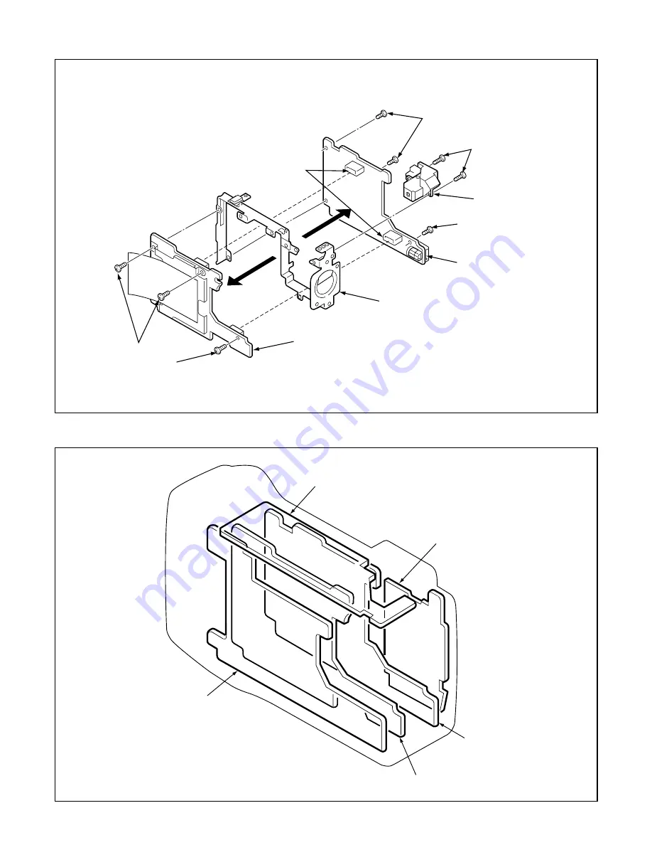
2-5. REMOVAL OF CA3 BOARD AND CA2 BOARD

2-6. BOARD LOCATION

CA1 board

SY1 board

PW1 board

CA2 board

CA3 board

1. Three screws
    1.7 x 2.5

7. CA2 board

8. Holder chassis M

2. Two screws
    1.7 x 4.0

3. Lens VF

4. Two screws
    1.7 x 2.5

5. Two connectors

4. Screw 1.7 x 2.5

6. CA3 board

Summary of Contents for VPC-SX 560

Page 1: ...ue are of special significance to product safety Should any component designated by a symbol need to be replaced use only the part designated in the Parts List Do not deviate from the resistance wattage and voltage ratings shown CAUTION Danger of explosion if battery is incorrectly replaced Replace only with the same or equivalent type recommended by the manufacturer Discard used batteries accordi...

Page 2: ...ESCRIPTION Around CCD block 1 IC Configuration IC903 ICX267 CCD imager IC902 IC904 IC908 74ACT04MTC H driver IC907 CXD3400N V driver IC905 AD9840 CDS AGC A D converter 2 IC903 CCD Structure Interline type CCD image sensor Optical size Diagonal 8 mm 1 2 type Effective pixels 1392 H 1040 V Pixels in total 1434 H 1050 V Actual pixels 1360 H 1024 V Optical black Horizontal H direction Front 2 pixels R...

Page 3: ...he reset gate clock 4 IC905 CDS AGC Circuit and A D Converter The video signal which is output from the CCD is input to Pin 30 of IC905 There are S H blocks inside IC905 generated from the XSHP and XSHD pulses and it is here that CDS correlated double sampling is carried out After passing through the CDS circuit the signal passes through the AGC amplifier It is A C converted internally into a 10 b...

Page 4: ...mes deep Thus the potential of the floating diffusion changes in proportion to the quantity of transferred electric charge and becomes CCD output after being received by the source follower The equivalent circuit for the output circuit is shown in Fig 1 7 H1 H2 H1 H2 H1 HOG RG CCD OUT PD Floating diffusion 1 H1 H2 H1 H2 H1 HOG RG CCD OUT PD 2 H1 H2 H1 H2 H1 HOG RG CCD OUT 3 H1 H2 RG CCD OUT 3 5V 0...

Page 5: ...crophone to 8 bit digital signals 1 9 8 bit A D circuit Audio The audio signals which were converted to digial form by the 8 bit A D circuit are temporarily to a sound buffer and then recorded in the SSFDC card During playback the 8 bit D A circuit converts these signals into analog audio signals 1 10 Sound buffer Audio memory 1 11 LCD driver The Y C signals which are input to the LCD driver are c...

Page 6: ...e way as for EE the data is then sent to the SDRAM after which D A conversion is carried out inside the ASIC and then the data is sent to the LCD panel and displayed The LCD driver is converted Y C signals to RGB signals from ASIC and these RGB signals and the control signal which is output by the LCD driver are used to drive the LCD panel The RGB signals are 1H transposed so that no DC compo nent...

Page 7: ... is necessary for controlling the power supply for a PWM type switching regulator and is pro vided with one built in channel Feedback from 10 mA L power supply output is received and the PWM duty is varied so that each one is maintained at the correct current setting level 3 1 Protection circuit If output is short circuited for the length of time determined by the condenser which is connected to P...

Page 8: ...h of time determined by the condenser which is connected to Pin 17 of IC501 all output is turned off The control signal P ON P A ON and LCD ON are recontrolled to restore output 3 Digital 3 3 V Power Output 3 3 V D is output Feedback for the 3 3 V D is provided to the switching controller Pins 1 of IC501 so that PWM con trol can be carried out 4 Digital 3 4 V System Power Output 3 4 V D is output ...

Page 9: ... current which is generated at the secondary side of T5401 is rectified to produce a high voltage direct current and is accumulated at electrolytic ca pacitor C5412 on the main circuit board 1 6 Voltage monitoring circuit This circuit is used to maintain the voltage accumulated at C5412 at a constance level After the charging voltage is divided and converted to a lower voltage by R5417 and R5419 i...

Page 10: ...ta input ASIC Serial communication data output ASIC Serial communication clock output ASIC Connect to GND Main clock oscillation terminal Main clock oscillation terminal 4 MHz VDD Sub clock oscillation terminal Sub clock oscillation terminal 32 768 kHz Reset input Battery OFF detection signal L OFF RS 232C RXD input terminal Serial communication request signal L Request Key matrix output 1 6 SY1 C...

Page 11: ...ts The 8 bit microprocessor reads the signals from each sensor element as input data and outputs this data to the camera circuits ASIC or to the LCD display device as operation mode setting data Fig 4 1 shows the internal commu nication between the 8 bit microprocessor and ASIC 3 Key Operaiton For details of the key operation refer to the instruction manual 8 bit microprocessor ASIC S REQ ASIC TES...

Page 12: ...is carried out even when the power switch is turned off so that the camera can start up again When the battery is removed the 8 bit micro processor operates in sleep mode using the backup capacitor At this time the 8 bit microprocessor only carries out clock counting and waits in standby for the battery to be attached again When a switch is operated the 8 bit microprocessor supplies power to the s...

Page 13: ...wo screws 1 7 x 2 5 22 Holder card 16 Slide the cover jack 17 Two screws 1 7 x 3 0 14 Dec cabinet R 15 Holder bracket R 6 Cover card 1 Three screws 1 7 x 3 0 3 Three screws 1 7 x 3 0 5 Cabinet front 4 Connector 23 Dec cabinet L 12 Screw 1 7 x 2 5 11 Spacer holder F2 9 Screw 1 7 x 2 5 10 Cabinet top 8 Button info 13 FPC 2 Cabinet back 1 Five screws 1 7 x 3 0 7 Screw 1 7 x 4 0 18 Holder terminal 19 ...

Page 14: ...2 Two screws 1 7 x 3 0 2 Two screws 1 7 x 3 0 3 Remove the solders 4 Holder battery 5 Three screws 1 7 x 2 5 6 PW1 board 7 Holder chassis F 8 Spacer PW1 side A 1 Two screws 1 7 x 2 5 5 Holder chassis B 3 FPC 4 LCD 2 Connector 12 Three screws 1 7 x 2 5 10 Connector 6 FPC 11 CA1 board 9 FPC 7 Two screws 2 0 x 6 0 8 Screw 2 0 x 2 5 ...

Page 15: ...A2 BOARD 2 6 BOARD LOCATION CA1 board SY1 board PW1 board CA2 board CA3 board 1 Three screws 1 7 x 2 5 7 CA2 board 8 Holder chassis M 2 Two screws 1 7 x 4 0 3 Lens VF 4 Two screws 1 7 x 2 5 5 Two connectors 4 Screw 1 7 x 2 5 6 CA3 board ...

Page 16: ...ible PC with Pentium processor CD ROM drive 3 5 inch high density diskette drive Serial port with standard RS 232C interface or USB port 8 MB RAM Hard disk drive with at least 15 MB available VGA or SVGA monitor with at least 256 color display 2 Installing calibration software 1 Insert the calibration software installation diskette into your diskette drive 2 Open the explorer 3 Copy the DSC Cal fo...

Page 17: ...w on the USB cable connector with the notch on the camera s USB port Insert the connector 3 Line up the serial connector on the serial cable with the serial port on your computer and insert the connector In case of USB cable line up the USB connector on the USB cable with the USB port on your computer and insert the connector 4 Turn on the camera and your computer system AC adaptor USB cable Seria...

Page 18: ...ith VR506 to 12 40 0 05 V 7 AWB Adjustment Preparation POWER switch ON Adjusting method 1 When setting the camera in place set it to an angle so that nothing appears in any part of the color viewer except the white section Do not enter any light 2 Double click on the DscCalDi126 3 Click the AWB and click the Yes Measuring Point ADJ Location Measuring Equipment ADJ Value Q5006 1 2 5 6 Frequency cou...

Page 19: ...itch ON Set the camera mode Adjustment method 1 Double click on the DscCalDi126 2 Select CCD Defect Detection on the LCD Test and click the Yes 3 After the adjustment is completed OK will display 4 Click the OK 10 LCD Panel Adjustment CA3 board Side A 10 1 LCD H AFC Adjustment Preparation POWER switch ON Adjusting method 1 Double click on the DscCalDi126 2 Select 0 on the LCD H AFC 3 Apply the tri...

Page 20: ...ng method 1 Adjust LCD B Bright so that the amplitude of the CL171 waveform is VG 0 2 0 05 Vp p with respect to the CL173 VG waveform Note 10 2 LCD RGB Offset adjustment and 10 3 LCD Gain ad justment should always be carried out first CL173 waveform CL172 waveform VG 0 1 0 05 Vp p VG 10 5 LCD Red Brightness Adjustment Adjusting method 1 Adjust LCD R Bright so that the amplitude of the CL172 wavefo...

Page 21: ...ndow and check the USB storage data VID SANYO PID VPC SX560EX or VPC SX560E or VPC SX560 Serial Rev 1 00 4 Check the Serial in the above USB storage data If the displayed value is different from the serial number printed on the base of the camera enter the number on the base of the camera Then click the Set button 5 Next check VID PID and Rev entries in the USB storage data If any of them are diff...

Page 22: ...LATION CHECK IC111 9 L1106 SD CLK 57 MHz OSCILLATION IC106 107 38 SD RAM IC106 IC107 MOVEMENT CLOCK NO READ PROGRAM FROM IC121 IF ABSENT CHECK IC102 IC106 IC107 IC102 140 141 IC301 75 76 CHECK SOLDERING OF MEMORY PIN INCORRECT HANDSHAKING BETWEEN 8 BIT CPU AND RS 232C CHECK EACH INTERFACE PUSH SUTTER BUTTON IC301 2 3 SCAN IN 4 5 PULSE INPUT CHECK R3025 R3026 D3067 D3068 CN301 7 8 P ON P A ON CHECK...

Page 23: ...05 LABEL COVER CARD SX112 J 23 411 018 1802 SCR PAN PCS 1 7X2 5 24 636 057 5233 HOLDER CARD SX113 J 25 636 057 8371 COMPL COVER BATT SX113 J 26 636 054 7216 SPRING P COVER SX112 J 27 411 177 8407 SCR S TPG PAN PCS 1 7X3 28 636 058 2378 SHIELD TAPE 29 636 058 7762 SHIELD TAPE 30 636 058 1180 SPACER HOLDER F2 SX112 J 31 636 056 2523 HEAT SINK RUBBER A SX112J 32 636 054 7186 SHAFT STRAP SX112 J 33 63...

Page 24: ...112 J 26 636 056 2646 SPACER CHASSIS M SX112 J 27 636 059 2322 COMPL PWB CA 3 VPC SX560 ONLY 27 636 059 7631 COMPL PWB CA 3 EXCEPT VPC SX560 28 636 056 2653 SPACER LENS SX112 J 29 636 056 2615 ADHESIVE TAPE VF SR661 J 30 411 018 3707 SCR PAN PCS 1 7X4 31 645 028 1457 ASSY LENS VF 32 636 054 7155 REFLECTOR POWER SX112 J 33 636 055 4658 LABEL CAUTION BATT SX112J 34 636 054 6974 HOLDER SP HOOK SX112 ...

Page 25: ...V C9118 403 322 1005 CERAMIC 0 1U Z 16V C9119 403 283 5708 CERAMIC 2200P K 50V C9120 403 283 6309 CERAMIC 1U Z 10V C9121 403 296 1308 TA SOLID 10U M 20V C9122 403 322 1005 CERAMIC 0 1U Z 16V C9123 403 345 4304 TA SOLID 22U M 10V C9124 403 283 6309 CERAMIC 1U Z 10V C9125 403 283 6309 CERAMIC 1U Z 10V C9126 403 283 6309 CERAMIC 1U Z 10V C9127 403 276 1007 CERAMIC 0 01U K 16V C9130 403 322 1005 CERAM...

Page 26: ...P3232ECY IC138 409 466 6104 IC TC7W32FK IC139 409 149 5301 IC TC7S00F IC146 409 435 6906 IC SN74LV245AP IC147 409 435 6906 IC SN74LV245AP IC148 409 435 6807 IC SN74LV244AP IC149 409 435 6807 IC SN74LV244AP IC152 409 427 4101 IC TK15405M IC154 409 363 3206 IC TC7SH32FU IC161 409 395 5902 IC TC7SH00FU IC162 409 432 2505 IC LMV321M7X DIODES D1301 407 149 0807 DIODE 1SS355 D1501 407 109 4609 DIODE MA7...

Page 27: ...6 MT GLAZE 10K JA 1 16W R1092 401 224 9006 MT GLAZE 10K JA 1 16W R1093 401 224 9006 MT GLAZE 10K JA 1 16W R1103 401 226 1503 MT GLAZE 0 000 ZA 1 16W VPC SX560 ONLY R1104 401 226 1503 MT GLAZE 0 000 ZA 1 16W EXCEPT VPC SX560 R1108 401 105 7909 MT GLAZE 0 000 ZA 1 16W R1110 401 225 2006 MT GLAZE 680 JA 1 16W R1201 401 225 8107 MT GLAZE 10 JA 1 16W R1202 401 037 5004 MT GLAZE 0 000 ZA 1 10W R1322 401...

Page 28: ...AMIC 1U M 6 3V C5102 403 333 3708 CERAMIC 10U M 10V C5103 403 338 4403 CERAMIC 0 1U K 16V C5104 403 316 1400 CERAMIC 560P J 25V C5105 403 333 3708 CERAMIC 10U M 10V C5106 403 340 1803 CERAMIC 1U M 25V C5108 403 327 0300 CERAMIC 10U Z 25V C5109 403 157 3601 CERAMIC 100P J 50V C5201 403 338 4403 CERAMIC 0 1U K 16V C5202 403 338 4403 CERAMIC 0 1U K 16V C5203 403 338 4403 CERAMIC 0 1U K 16V C5204 403 ...

Page 29: ...EMI 1K S INDUCTORS L5001 645 036 5362 INDUCTOR 6 2U M L5002 645 033 8762 INDUCTOR 47U K L5003 645 033 8762 INDUCTOR 47U K L5004 645 033 8762 INDUCTOR 47U K L5006 645 021 5315 INDUCTOR 110 OHM L5007 645 030 5887 INDUCTOR 1000 OHM L5009 645 033 7918 INDUCTOR 10U M L5010 645 036 5362 INDUCTOR 6 2U M L5011 645 033 8663 INDUCTOR 10U K L5012 645 033 8663 INDUCTOR 10U K L5014 645 033 8663 INDUCTOR 10U K ...

Page 30: ...0 MT GLAZE 100K JA 1 16W R5061 401 262 2304 MT GLAZE 1 0K DC 1 16W R5062 401 224 9402 MT GLAZE 1 0M JA 1 16W R5063 401 224 9402 MT GLAZE 1 0M JA 1 16W R5064 401 262 5206 MT GLAZE 1 5K DC 1 16W R5065 401 258 9102 MT GLAZE 5 6K DC 1 16W R5066 401 258 9300 MT GLAZE 220K DC 1 16W R5067 401 258 0406 MT GLAZE 120K DC 1 16W R5068 401 224 9402 MT GLAZE 1 0M JA 1 16W R5069 401 274 9704 MT GLAZE 24K DC 1 16...

Page 31: ...JA 1 16W R3005 401 105 5400 MT GLAZE 47K JA 1 16W R3006 401 105 5400 MT GLAZE 47K JA 1 16W R3007 401 105 0603 MT GLAZE 10K JA 1 16W R3010 401 105 5400 MT GLAZE 47K JA 1 16W R3011 401 167 2508 MT FILM 100K DD 1 16W R3012 401 167 2508 MT FILM 100K DD 1 16W R3014 401 105 0702 MT GLAZE 100K JA 1 16W R3015 401 105 5400 MT GLAZE 47K JA 1 16W R3016 401 105 0603 MT GLAZE 10K JA 1 16W R3017 401 105 0702 MT...

Page 32: ...7129 CABLE MINI 8P D SUB 9P EXCEPT VPC SX560E 3 Adapter for Macintosh computer 645 040 2807 CABLE DSC USB 4 USB interface cable 636 057 8968 CASE SOFT SX113 J 636 056 1007 STRAP HAND SR662 J 645 037 2322 CARD CF CompactFlash EXCEPT VPC SX560E 645 037 2339 CARD CF CompactFlash EXCEPT VPC SX560E 645 043 5553 DISC CD ROM CEL SUSP52 E Sanyo Software Pack 5 2 645 043 5546 DISC CD ROM MGI MGI PhotoSuite...

Page 33: ...OVERALL WIRING ...

Reviews: