background image

– 11 –

2. DISASSEMBLY

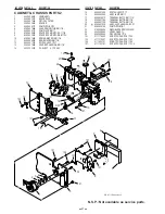
2-1. REMOVAL OF CABINET BACK, CABINET FRONT, TB1 BOARD AND LCD

1. Open the cover battery.

2. Four screws 1.7 x 4

3. Open the cover card.

4. Four screws 1.7 x 6

5. Cabinet back

6. Screw 1.7 x 4

7. Screw 1.7 x 6

8. Cabinet top A

9. Cabinet front

10. Cover battery

11. Cover card

12. Shaft card

13. Screw 1.7 x 3.5

14. TB1 board

15. Spacer CV monitor 2

16. FPC

17. Remove the solder.

18. LCD

19. Three screws 1.7 x 4

20. Holder monitor

1

2

2

3

4

4

5

6

7

8

9

2

10

11

12

A

B

C

D

E

F

G

H

13

14

16

17

18

19

20

brown

yellow

gray

pink

white

white

pink

15

The order of tighting screws

A

B

C

D

E

F

G

H

When assembling cabinet front

1. The cover lens should be closed.

2. Set the knob macro at the normal position.

Summary of Contents for VAR-G5E

Page 1: ...ol need to be replaced use only the part designated in the Parts List Do not deviate from the resistance wattage and voltage ratings shown CAUTION Danger of explosion if battery is incorrectly replaced Replace only with the same or equivalent type recommended by the manufacturer Discard used batteries according to the manufacturer s instructions NOTE 1 Parts order must contain model number part nu...

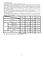
Page 2: ...al 4 Table 1 1 CCD Pin Description 10 12 51 2 H V 1 2 23 24 3 4 5 6 7 12 17 18 19 20 21 22 PI1 PI2 PI3 PI4 NC PW PR VSUB PS4 PS3 Image clock Accumulation clock Reset gate N substrate Image clock Accumulation clock P well DC 0 12 V PS1 PS2 0 12 V 0 12 V L 18 V H 23 V DC 8 V CCD output gate VOG 3 3 V Frame shift Frame shift Line sending 8 VOUT CCD output 9 VDD Power 10 VSS GND 11 VRD Reset drain DC ...

Page 3: ...ut to Pins 26 and 27 of IC901 There are S H blocks inside IC905 generated from the XSHP and XSHD pulses and it is here that CDS correlated double sampling is carried out After passing through the CDS circuit the signal passes through the AGC amplifier It is A C converted internally into a 10 bit signal and is then input to IC102 Fig 1 5 IC901 Block Diagram 27 29 36 26 16 22 21 30 23 19 11 12 17 PB...

Page 4: ...usion PR is then turned on again by the timing in 1 when the H2 potential becomes deep Thus the potential of the floating diffusion changes in proportion to the quantity of transferred electric charge and becomes CCD output after being received by the source follower The equivalent circuit for the output circuit is shown in Fig 1 7 6 Lens drive block 6 1 Shutter drive The regulator IC952 drives by...

Page 5: ...age fixed at DC and the R G and B signals becomes greater the display becomes darker if the difference in potential is smaller the element opens and the LCD become brighter In addition the bright ness and contrast settings for the LCD can be varied by means of the serial data from the ASIC 1 2 CA B CIRCUIT DESCRIPTION 1 Circuit description 1 1 PTG This is program timing generator Generates the tim...

Page 6: ...ed to Pin 29 of IC501 all output is turned off The control signal P ON are recontrolled to restore output 3 Digital 3 4 V Power Output 3 4 V D is output Feedback is sent to pin 41 of the switch ing controller IC501 for PWM control to be carried out 4 Digital 5 V and Analog System Power Output 5 1 V D 26 4 V A 20 V A 13 V A and 5 1 V A are output Feedback for the 5 1 V D is provided to the switch i...

Page 7: ...age alternating current which is generated at the secondary side of T5401 is rectified to produce a high voltage direct current and is accumulated at electrolytic ca pacitor C5412 on the main circuit board 1 6 Voltage monitoring circuit This circuit is used to maintain the voltage accumulated at C5412 at a constance level After the charging voltage is divided and converted to a lower voltage by R5...

Page 8: ...ower Analog power Main ASIC system power detection Battery power input analog input Main ASIC system power detection Connect to GND through register AC adaptor connection detection analog input Main clock oscillation terminal 4 MHz Connect to GND Reset input Key matrix input Connect to GND through register Connect to GND through register ASIC PLL permission signal USB connection detection H Connec...

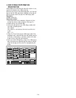
Page 9: ...uts this data to the camera circuits ASIC or to the LCD display device as operation mode setting data Fig 4 1 shows the internal communication between the 8 bit microprocessor ASIC and SPARC lite circuits 3 Key Operaiton For details of the key operation refer to the instruction manual 8 bit Microprocessor ASIC REQACK EXT_IRQ1 SDATA SDIR SCK RESET B 0 1 2 0 1 2 3 SCAN OUT SCAN IN MAIN SW PLAY POSIT...

Page 10: ...a can start up again When the battery is removed the 8 bit micro processor operates in sleep mode using the backup capacitor At this time the 8 bit microprocessor only carries out clock counting and waits in standby for the battery to be attached again When a switch is operated the 8 bit microprocessor supplies power to the system as required The 8 bit microprocessor first sets the P ON signal at ...

Page 11: ...ck the USB storage data VID SANYO PID VPC R1 or VPC R1E or VPC R1EX or VPC R1G Serial Rev 1 00 4 Check the Serial in the above USB storage data If the displayed value is different from the serial number printed on the base of the camera enter the number on the base of the camera Then click the Set button 5 Next check VID PID and Rev entries in the USB storage data If any of them are different from...

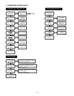
Page 12: ...28 63636MHz OSCILLATION CHECK X1102 SD CLK 57 27 MHz OSCILLATION IC103 38 SD RAM IC103 MOVEMENT CLOCK NO READ PROGRAM FROM IC121 IF ABSENT CHECK IC102 IC103 IC102 237 IC301 39 40 CHECK SOLDERING OF MEMORY PIN INCORRECT HANDSHAKING BETWEEN 8 BIT CPU AND RS 232C CHECK EACH INTERFACE PUSH SHUTTER BUTTON IC301 20 21 SCAN IN 0 1 PULSE INPUT CHECK RB301 D3006 D3007 CN301 34 P ON CHECK IC301 POWER BLOCK ...

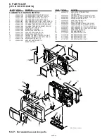
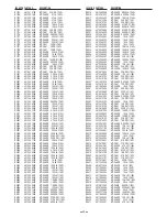
Page 13: ...B117 U EXCEPT VPC R1G 11 636 063 2189 SPRING SHUTTER SB117 U 12 636 064 2997 ASSY BUT SHUTTER SB117 U EXCEPT VPC R1G 12 636 064 3147 ASSY BUT SHUTTER SB117EX2 VPC R1G ONLY 13 636 064 3444 CABINET TOP A SB117 EX2 VPC R1G ONLY 13 636 062 7604 CABINET TOP A SB117 U EXCEPT VPC R1G 14 636 063 1625 SPACER MONITOR SB117 U 15 636 062 8335 SLIDE FUNCTION SB117 U 16 636 063 1632 SHAFT CARD SB117 U 17 636 06...

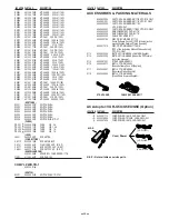
Page 14: ... HOLDER CHASSIS B SB117 U 14 403 324 3502 DL ELECT 0 1F Z 5 5V 15 645 025 1252 SWITCH LEAF 1P 1T 16 645 048 9969 ASSY LAMP SB117 17 636 063 0918 TERMINAL BATT C SB117 U 18 636 062 7765 TERMINAL BATT B SB117 U 19 636 062 7758 TERMINAL BATT A SB117 U 20 636 065 1838 ASSY HLD CHASSIS A SV 117 21 636 062 8144 COMPL PWB TB 1 22 419 002 6604 PIEZO BUZZER PS1550L40N 23 645 049 8664 LENS VF ASSY 24 636 06...

Page 15: ...109 Q5407 405 115 5207 TR 2SC4617 R Q5409 405 158 0306 TR CY25AAJ 8 Q9001 405 133 8907 TR DTC114EUA OR 405 119 0802 TR UN5211 OR 405 078 7300 TR 2SC4398 Q9002 405 165 7305 TR BFR92AW Q9003 405 102 5500 TR 2SB1218A R OR 405 137 2000 TR 2SA1576A R INTEGRATED CIRCUITS IC102 409 509 6504 IC CX11637 21 BGA N S P IC103 409 482 0506 IC HY57V651620BTC 10S OR 409 502 3807 IC HY57V641620HGT H IC106 409 484 ...

Page 16: ... 5P C 50V C1103 403 309 8102 CERAMIC 5P C 50V C1104 403 311 7803 CERAMIC 8P D 50V C1105 403 311 7803 CERAMIC 8P D 50V C1201 403 332 9503 CERAMIC 1U M 6 3V C1301 403 311 5809 CERAMIC 47P J 50V C1302 403 311 5809 CERAMIC 47P J 50V C1401 403 312 6805 CERAMIC 0 1U Z 16V C1402 403 312 6805 CERAMIC 0 1U Z 16V C1403 403 312 6805 CERAMIC 0 1U Z 16V C1412 403 312 6805 CERAMIC 0 1U Z 16V C1502 403 324 0501 ...

Page 17: ...49 403 312 6805 CERAMIC 0 1U Z 16V C9050 403 338 4403 CERAMIC 0 1U K 16V C9051 403 213 5501 ELECT 10U M 25V C9052 403 312 6805 CERAMIC 0 1U Z 16V C9053 403 164 0204 CERAMIC 0 1U Z 25V C9054 403 164 0204 CERAMIC 0 1U Z 25V C9056 403 218 4905 ELECT 4 7U M 35V C9057 403 312 6805 CERAMIC 0 1U Z 16V C9058 403 164 0204 CERAMIC 0 1U Z 25V C9059 403 280 3400 ELECT 47U M 35V C9501 403 338 4403 CERAMIC 0 1U...

Page 18: ...ZE 0 000 ZA 1 16W R5012 401 267 6604 MT GLAZE 270K DC 1 16W R5013 401 267 6604 MT GLAZE 270K DC 1 16W R5014 401 240 9608 MT GLAZE 680K JA 1 16W R5015 401 240 9608 MT GLAZE 680K JA 1 16W R5016 401 226 1503 MT GLAZE 0 000 ZA 1 16W R5017 401 224 9402 MT GLAZE 1 0M JA 1 16W R5020 401 261 3906 MT FILM 2 2K DU 1 16W R5021 401 261 8703 MT FILM 22K DD 1 16W R5022 401 267 6604 MT GLAZE 270K DC 1 16W R5025 ...

Page 19: ...006 645 045 2857 SWITCH PUSH S3008 645 029 5812 SWITCH SLIDE 1P 3T FUSES PR501 423 028 0904 FUSE 32V 2A PR502 423 028 1307 FUSE 32V 1 5A PR503 423 028 1505 FUSE 32V 1A PR504 423 028 1505 FUSE 32V 1A JACK JK501 645 050 0817 SOCKET DC CONNECTORS CN110 645 049 1405 SOCKET USB 5P CN141 645 050 8431 PLUG CARD 50P N S P CN171 645 004 7183 SOCKET FPC 24P N S P CN951 645 037 6139 SOCKET FFC 6P N S P MISCE...

Page 20: ...ont 10 Cover battery 11 Cover card 12 Shaft card 13 Screw 1 7 x 3 5 14 TB1 board 15 Spacer CV monitor 2 16 FPC 17 Remove the solder 18 LCD 19 Three screws 1 7 x 4 20 Holder monitor 1 2 2 3 4 4 5 6 7 8 9 2 10 11 12 A B C D E F G H 13 14 16 17 18 19 20 brown yellow gray pink white white pink 15 The order of tighting screws A B C D E F G H When assembling cabinet front 1 The cover lens should be clos...

Page 21: ... yellow white 4 5 6 blue gray pink violet TB1 board CP1 board 1 Screw 1 7 x 3 2 Two screws 1 7 x 4 3 Holder chassis B 4 DL elect 5 Screw 1 7 x 3 6 Switch leaf 7 Three screws 1 7 x 4 8 Two screws 1 7 x 5 9 FPC 10 CP1 board 7 10 8 9 red red black gray black red black black red CCD Lens ...

Page 22: ...ng USB drive Install the USB drive with camera or connection kit for PC 4 Color Viewer 1 Turn on the switch and wait for 30 minutes for aging to take place before using Color Pure 2 The luminance adjustment control on the color viewer should be set to around the middle position memory 5 during use 3 The fluorescent lamps which are used in the color viewer are consumable parts After the cumulative ...

Page 23: ...red jig connection point 1 Line up the arrow on the cable connector with the notch on the camera s USB port Insert the connector 2 Locate a USB port on your computer AC adaptor To USB port USB cable GND V OUT VDD3 Picutured jig connection point CP1 board side B ...

Page 24: ...no operational problems in the com puter in taking still pictures in a set condition 11 Pull the DC jack to turn off the camera after completing the adjustment and pull the CF card 12 Remove the lead of the pictured jig Confirm that there are no operational problems in taking still pictures in a set condition 13 When this adjustment is carried out it is necessary to per form the 3 CCD adjustment a...

Page 25: ...the 3 CCD adjustment and 4 Strobe adjust ment after completing the LCD adjustment Adjustment method 1 Copy all the CCD calibration files to the CF card 2 Click on Cmdfile txt to activate the name field in the CF card and push the enter key to change the name to lcdcal using all lower case letters Click the save button to save 3 Set the CF card which is saved to the camera 4 Put DC jack to the came...

Page 26: ...LCD Gain adjust ment have done CL415 waveform CL414 waveform VG VG 0 1 Vp p CL415 waveform CL413 waveform VG VG 0 1 Vp p 5 4 LCD Red Brightness Adjustment Adjusting method 1 Adjust LCD R Bright so that the amplitude of the CL414 waveform is VG 0 1 Vp p with respect to the CL415 VG waveform Note 5 2 LCD RGB Offset adjustment and 5 3 LCD Gain adjust ment should always be carried out first CL415 wave...

Reviews: