background image

-  2  -

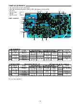
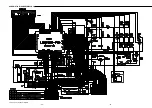
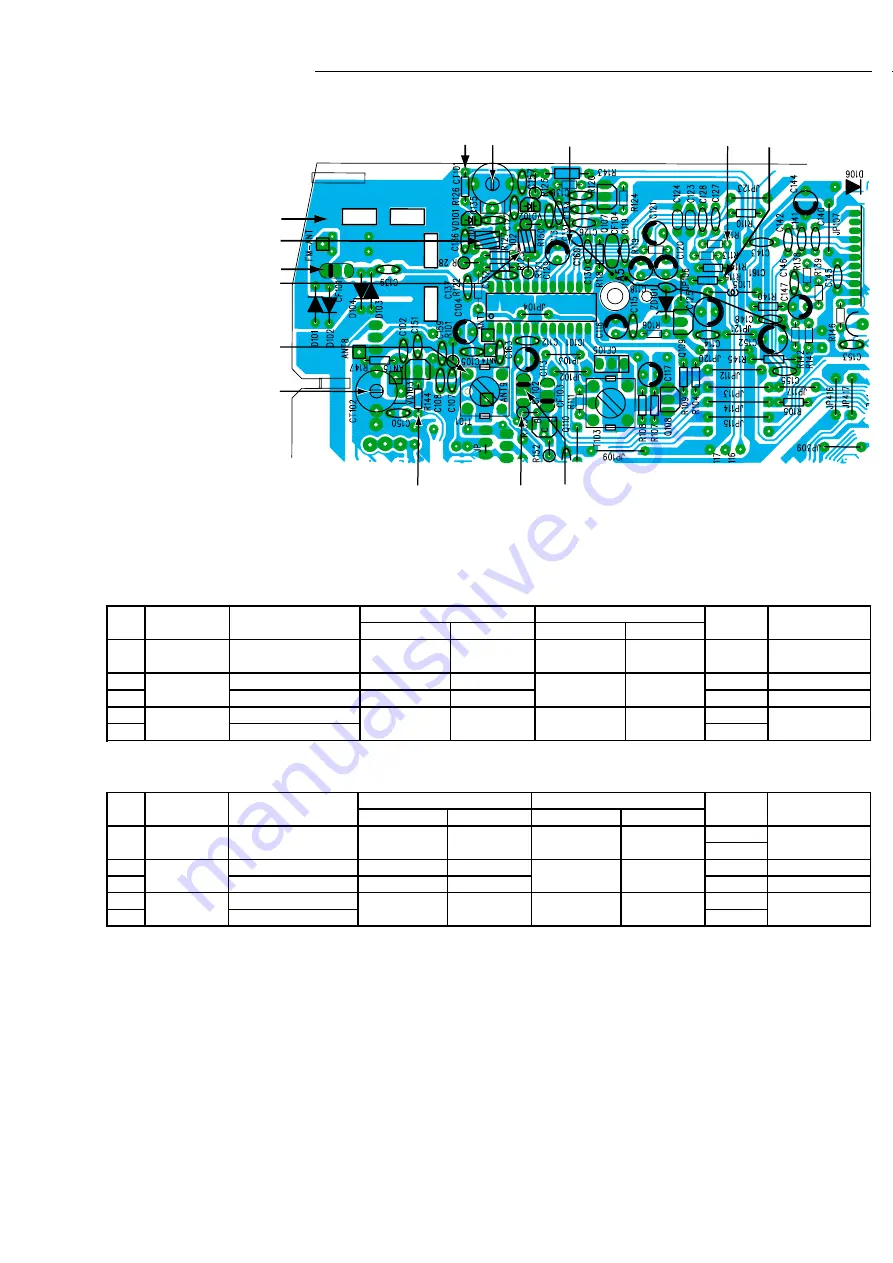
TP4

TP3

TP7

CT102

T101

L102

TP1

L101

TP2

TP6 CT101

TP5

TP8

TP9

• Use a plastic screw driver for adjustments.
• Adjust the intermediate frequency of AM and FM to the frequency of ceramic filter.
• Set of unit

Supply voltage

: DC 12V

Speaker

: 32 

Function switch

: RADIO

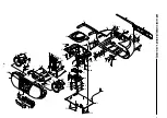
PARTS LOCATION

TUNER ADJUSTMENTS

This is a basic adjustment.

1. AM ADJUSTMENT

Step

Adjusting

Tuning

Adjust-

VTVM

Circuit

Frequency

Instrument

Input

Instrument

Output

ment

Oscilloscope

1

IF

999 KHz

AM  sweep

Loop ANT.

VTVM

Speaker

T103

Max.

(450 KHz)

generator

oscilloscope

2

Tuning

522 KHz

---

---

Digital

TP7(H)

T101

1.5V

±

0.05V

3

coverage

1611  KHz

---

---

voltmeter

TP2(E)

---

7.4V

±

0.1V

4

Tracking

603 KHz

AM signal

Loop ANT.

VTVM

Speaker

AM COIL

Max.

5

1404 KHz

generator

oscilloscope

CT102

Input Connection

Output Connection

1. FM ADJUSTMENT

BAND SELECT SWITCH : FM

FM Dummy Antenna:75

 unbalance

Step

Adjusting

Tuning

Adjust-

VTVM

Circuit

Frequency

Instrument

Input

Instrument

Output

ment

Oscilloscope

1

IF

98.0MHz

FM sweep

TP3(H)

VTVM

TP5(H)

---

Non Adjustment

10.7NHz

generator

TP4(E)

oscilloscope

TP4(E)

2

Tuning

87.5Hz

---

---

Digital

TP6(H)

L102

2.0V

±

0.1V

3

coverage

108.0MHz

---

---

voltmeter

TP2(E)

---

7.2V

±

0.1V

4

Tracking

90.0.MHz

FM signal

TP1(H)

VTVM

TP8(H)

L101

Max.

5

106.0MHz

generator

TP2(E)

oscilloscope

TP9(E)

CT103

Input Connection

Output Connection

Summary of Contents for 164 081 00

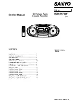
Page 1: ...recaution 1 Tuner Adjustment 2 Tape Deck Adjustment 3 IC Block Diagram Description 3 7 Exploded View Cabinet Chassis 4 Parts List 5 Exploded View Parts List Tape Deck 7 Wiring Connection 11 Schematic Diagram Micom 12 Schematic Diagram CD 14 Schematic Diagram Radio 16 Schematic Diagram Audio 18 Wiring Diagram CD Main Amp Tu 20 Wiring Diagram Rectifier Display Power 21 ...

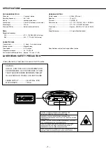
Page 2: ...PUT 0 6 mW Max CW WAVE LENGTH 790 nm LASER BEAM SAFETY PRECAUTION GENERAL SECTION Output power 3 W ch DC max Speaker 10 cm X 2 Terminal PHONE 32 Power source AC 110 120 220 240 V 50 60 Hz DC 12V 8 R20 D batteries Dimensions Approx 480 W x 167 H x 258 D mm Weight approx 3 0 kg without batteries Specifications subject to change without notice CAUTION INVISIBLE LASER RADIATION WHEN OPEN AND INTERLOCK...

Page 3: ...ing 522 KHz Digital TP7 H T101 1 5V 0 05V 3 coverage 1611 KHz voltmeter TP2 E 7 4V 0 1V 4 Tracking 603 KHz AM signal Loop ANT VTVM Speaker AM COIL Max 5 1404 KHz generator oscilloscope CT102 Input Connection Output Connection 1 FM ADJUSTMENT BAND SELECT SWITCH FM FM Dummy Antenna 75Ω unbalance Step Adjusting Tuning Adjust VTVM Circuit Frequency Instrument Input Instrument Output ment Oscilloscope ...

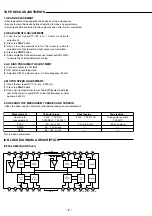
Page 4: ...n Cassette for PLAY TW 211A PLAY TW 2111A Drive power cassete measurement F FW REW TW 2231 TW 2412 PLAY 30 60 gr cm 2 0 4 5 gr cm 60 gr or more F FWD 55 120 gr cm REW 55 120 gr cm 1 HEAD REPLACEMENT After replacement demagnetize the heads by using a degausser Be sure to clean the heads before attempting to make any adjustments All wiring should be returned to the original position after work is co...

Page 5: ...7 8 Y01 Y01 Y02 Y04 Y05 Y09 Y09 Y14 Y16 Y17 Y15 Y18 Y18 Y18 60 Y20 Y20 Y18 Y21 Y18 Y18 Y10 Y11 Y11 Y12 Y13 Y13 Y12 Y03 Y03 8 9 51 51 52 53 71 72 15 14 17 18 19 21 23 27 28 29 31 74 56 73 32 33 58 59 57 34 38 32 30 54 55 26 16 11 4 39 40 Y06 ...

Page 6: ...ION Y01 645 027 1168 SCR 3X8 SPK Y02 645 023 6624 SCREW ST 3X10 POWER KNOB Y03 645 023 6617 SCREW ST 3X10 CD CTL BD Y04 645 027 1168 SCR 3X8 CASS DOOR GEAR Y05 645 023 6617 SCREW ST 3X10 CASS DECK Y06 645 027 1168 SCR 3X8 CD DOOR GEAR Y10 645 033 4276 SCR 2X6 CD MICRO SW Y11 645 027 1373 WASHER METAL Y12 645 033 0247 SCR 2 6X8 CD DECK Y13 645 023 6594 SCREW ST 3X8 MAIN BD Y14 645 027 1182 SCR 3X20...

Page 7: ...D0101 645 055 6821 DIODE 1N4148 D0102 645 055 6821 DIODE 1N4148 D0103 645 055 6821 DIODE 1N4148 D0104 645 055 6821 DIODE 1N4148 D0105 645 055 6821 DIODE 1N4148 D0106 645 055 6821 DIODE 1N4148 D0301 645 055 6821 DIODE 1N4148 D0302 645 055 6821 DIODE 1N4148 D0303 645 023 6112 RECTIFIER 1N 4001 D0304 645 055 6821 DIODE 1N4148 D0305 645 055 6821 DIODE 1N4148 D0306 645 055 6821 DIODE 1N4148 D0307 645 0...

Page 8: ...T GND IC BLOCK DIAGRAM DESCRIPTION RECTIFIER P W BOARD ASSY REF NO PART NO DESCRIPTION 74 614 324 1867 ASSY PWB RECTIFIER Only initial D1101 645 023 6112 RECTIFIER 1N 4001 D1102 645 023 6112 RECTIFIER 1N 4001 D1103 645 023 6112 RECTIFIER 1N 4001 D1104 645 023 6112 RECTIFIER 1N 4001 D1105 645 055 6821 DIODE 1N4148 F1101 645 055 7149 FUSE GLASS TUBE FS1101 645 035 0511 FUSE HOLDER MW1010K 645 042 03...

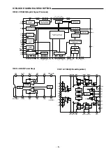
Page 9: ...FM Demodulation VCO Clock Oscillator Clock Control X tal Root Timing Generator RAM Address Generatorl 2K 8bit RAM Billingual Digital Out General Ports Digital Attenuator Quadruple Over Sampling Digital Filter Interpolalation Mute C1 C2 Error Detect Correct Control Flag 1bit DAC L P F CLV Digital Servo COM Inter Fase Servo Commander CONTROL CIRCUIT LOGIC CIRCUIT CCB INTERFACE CONTROL CIRCUIT 15 14 ...

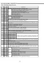
Page 10: ...l for digital signals Generalized I O terminal 1 Generalized I O terminal 2 Generalized I O terminal 3 Generalized I O terminal for command identification Pull down resistor incorporated When used as the same functi as LC78622E open circuit or ground H position enables only generalized I O command to be controlled L pos enables all the commands to be controlled Controlled by a serial data command ...

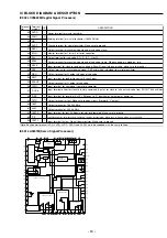
Page 11: ... of sub code Output terminal for synchronizing signals of sub code frame When sub code is stood by falls Input terminal for clock to read out sub code Schmitt input when not used make sure to ground Output terminal for synchronizing signal 7 35 kHz which is divided from crystal oscillator Output terminal for Q output standby of sub code Ground terminal for crystal oscillator Make sure to ground Ou...

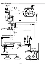
Page 12: ... YELLOW BLACK BROWN BROWN MOTOR SWITCH R P HEAD M CD MECHANISM CN101 15P CN403 3P CN201 5P CN903 13P CN301 4P CN901 16P CN401 3P CN902 6P CN904 2P JK301 PICKUP 16P CD MAIN AMP TU P W B CD SWITCH L CH SPEAKER R CH SPEAKER TAPE DECK MECHANISUM FM ROD ANT AC1 DC DC 12V DC 12V AC2 BLACK BLACK BLACK RED YELLOW WHITE ORANGE RED RED BLACK FS1101 T1 6A L 250V 6P ...

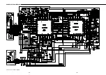
Page 13: ... 13 12 SCHEMATIC DIAGRAM DISPLAY This is a basic schematic diagram ...

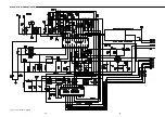
Page 14: ... 15 14 SCHEMATIC DIAGRAM CD This is a basic schematic diagram ...

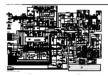
Page 15: ... 17 16 SCHEMATIC DIAGRAM TUNER This is a basic schematic diagram ...

Page 16: ...nated components in which safety can be of special significance When replacing a component identified by use only the replacement parts designated or parts with the same ratings of resistance wattage or voltage that are designated in the parts list in this manual Leakage current or resistance measurements must be made to determine that exposed parts are acceptably insulated from the supply circuit...

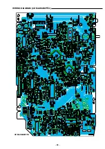
Page 17: ... 20 WIRING DIAGRAM CD MAIN AMP TU CD MAIN AMP TU ...

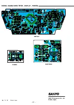
Page 18: ... 21 DISPLAY POWER RECTIFIER WIRING DIAGRAM RECTIFIER DISPLAY POWER May 02 BB Printed in Japan SANYO Technosound Co Ltd Osaka Japan ...

Reviews: