


Samsung Electronics
4-25
Alignment and Adjustment
8. Pre white balance (II)
1) Camera “E-E”, 3100°K gray-scale chart.
2) Video(output) jack and AF MICOM.
4) Connect vectorscope input jack to video(out-
put) jack.
3) Press the “FADE (MODE UP)/BLC(MODE
DOWN)” button so that the OSD state is “138.
XX XX”.
5) Aim the camera at a 3100°K gray-scale chart
illuminated at 1500 to 2000 lx.
6) Adjust the “TITLE(DATA UP)/Z.RETURN
(DATA DOWN)” button so that the white vec-
tor moves to the R-Y axial on screen of the vec-
torscope.
Note :
Bright dot shifts after the confirm button is
pressed.
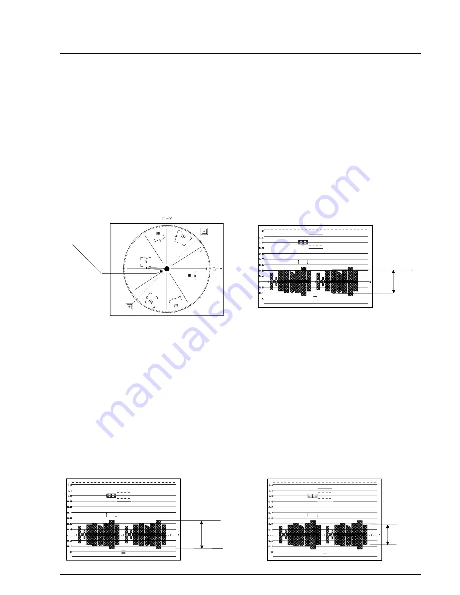
9 R-Y Positive Gain
1) Camera “E-E”, 3100°K color bar chart.
2) Video(output) jack and register of EEPROM.
3) Connect video(output) jack to waveform moni-
tor input jack and monitor TV jack respectively.
4) Press the “FADE(MODE UP)/BLC(MODE
DOWN)” button so that the OSD state is “147.
XX XX”.
5) Aim the camera at a color bar chart illuminated
at 1500 to 2000 lx.
6) Adjust the “ TITLE(DATA UP)/Z.RETURN(DATA
DOWN)” button so that the red level is 70IRE.
7) Be sure to press the “MENU ON/OFF(CON-
FIRM)” button to memorize setting.
Note :
Bright dot shifts after the confirm button is
pressed.
10. R-Y Negative Gain
1) Camera “E-E”, 3100°K color bar chart.
2) Video(output) jack and register of EEPROM.
3) Connect video(output) jack to waveform moni-
tor input jack and monitor TV jack respectively.
4) Press the “FADE(MODE UP)/BLC(MODE
DOWN)” button so that the OSD state is “148.
XX XX”.
5) Aim the camera at a color bar chart illuminated
at 1500 to 2000 lx.
6) Adjust the “ TITLE(DATA UP) /Z.RETURN(DATA
DOWN)” button so that the cyan level is 65IRE.
7) Be sure to press the “MENU ON/OFF(CON-
FIRM)” button to memorize setting.
Note :
Bright dot shifts after the confirm button is
pressed.
11. B-Y Positive Gain
1) Camera “E-E”, 3100°K color bar chart.
2) Video(output) jack and register of EEPROM.
3) Connect video(output) jack to waveform moni-
tor input jack and monitor TV jack respectively.
4) Press the “FADE(MODE UP)/BLC(MODE
DOWN)” button so that the OSD state is “14B
XX XX”.
5) Aim the camera at a color bar chart illuminated
at 1500 to 2000 lx.
6) Adjust the “TITLE(DATA UP)/Z.RETURN
(DATA DOWN)” button so that the blue level is
50IRE.
7) Be sure to press the “MENU ON/OFF(CON-
FIRM)” button to memorize setting.
Match the white luminance
point with the
black luminance
point
70IRE
65IRE
50IRE
Summary of Contents for VP-M50
Page 12: ...8 1 Samsung Electronics 8 Wiring Diagram ...
Page 16: ...9 4 Samsung Electronics Schematic Diagrams 9 1 DC DC Converter Main ...
Page 17: ...9 5 Samsung Electronics Schematic Diagrams 9 2 System Control Servo Main ...
Page 18: ...9 6 Samsung Electronics Schematic Diagrams 9 3 Video Normal Main ...
Page 19: ...9 7 Samsung Electronics Schematic Diagrams 9 4 Video Hi8 Main ...
Page 20: ...9 8 Samsung Electronics Schematic Diagrams 9 5 Audio Main ...
Page 21: ...9 9 Samsung Electronics Schematic Diagrams 9 6 Camera Main ...
Page 22: ...9 10 Samsung Electronics Schematic Diagrams 9 7 Rear ...
Page 23: ...9 11 Samsung Electronics Schematic Diagrams 9 8 CCD ...
Page 24: ...9 12 Samsung Electronics Schematic Diagrams 9 9 CVF ...
Page 25: ...9 13 Samsung Electronics Schematic Diagrams 9 10 Front ...
Page 26: ...9 14 Samsung Electronics Schematic Diagrams 9 11 Function ...
Page 27: ...9 15 Samsung Electronics Schematic Diagrams 9 12 EVF ...
Page 28: ...8 2 Samsung Electronics Wiring Diagram MEMO MEMO ...
Page 29: ...7 2 Samsung Electronics PCB Diagrams 7 1 Main PCB Normal Component Side ...
Page 30: ...7 3 Samsung Electronics PCB Diagrams ...
Page 31: ...7 4 Samsung Electronics PCB Diagrams 7 2 Main PCB Normal Conductor Side ...
Page 32: ...7 5 Samsung Electronics PCB Diagrams ...
Page 33: ...7 6 Samsung Electronics PCB Diagrams 7 3 Main PCB Hi8 Component Side ...
Page 34: ...7 7 Samsung Electronics PCB Diagrams ...
Page 35: ...7 8 Samsung Electronics PCB Diagrams 7 4 Main PCB Hi8 Conductor Side ...
Page 36: ...7 9 Samsung Electronics PCB Diagrams ...
Page 37: ...7 10 Samsung Electronics PCB Diagrams 7 5 Rear PCB Component Side Conductor Side VP M54 only ...
Page 38: ...7 11 Samsung Electronics PCB Diagrams 7 6 CCD PCB Component Side Conductor Side ...
Page 39: ...7 12 Samsung Electronics PCB Diagrams 7 7 CVF PCB Component Side Conductor Side ...
Page 40: ...7 13 Samsung Electronics PCB Diagrams 7 8 EVF PCB Component Side Conductor Side ...
Page 41: ...7 14 Samsung Electronics PCB Diagrams 7 9 Function PCB Component Side Conductor Side ...
Page 42: ...7 15 Samsung Electronics PCB Diagrams 7 10 Front PCB ...
Page 43: ...MEMO MEMO 7 16 Samsung Electronics PCB Diagrams ...
Page 61: ...Samsung Electronics 5 18 Exploded View and Parts List MEMO MEMO ...
Page 103: ...Samsung Electronics 3 12 Disassembly and Reassembly MEMO MEMO ...
Page 105: ...MEMO MEMO Products Specifications and Comparison Chart Samsung Electronics 2 4 ...


