background image

Alignment and Adjustments

4-16

Samsung Electronics

7.

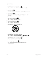
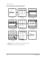
Use the           key for overall balance.

8.

After the Line Shift is cancelled by pressing the           key, use the Channel

and Volume keys (Up/Down) to make big adjustments.

9.  After the green convergence adjustments are completed, press the 

key to

save the data (The minor adjustments can be done only when adjusting Red and Blue).

Summary of Contents for Tantus PCK 6115R

Page 1: ...CE GUIDE Last update 3 14 01 Supercedes and appends service manual data Covers Models P51 Chassis PCJ612R PCJ 522R covers PCK520 PCJ533R PCJ533RF PCJ534RF covers PCJ532RF PCK5315R PCJ614RF covers PCJ611RF PCK6115R HCJ552W HCJ652W ...

Page 2: ... TV SERVICE GUIDE Last update 3 14 01 Table of Contents Sections 1 How to Use This Guide 2 Service Bulletins 3 Flow Charts Micro Kits 4 Macro Kit Instructions 5 Parts Data 6 Assembly Disassembly 7 Escalation Who to Call ...

Page 3: ...setup 4 If the previous steps do lead to a clear diagnosis then proceed to the flow chart in section 3 to help assist you in determining the correct PCB s to order 5 Place order through Samsung Parts Department Note Distributors DO NOT carry PCB s or macro kits so backorder with no eta will result Parts Department will not accept an order for PTV parts without a serial number because correct ID ca...

Page 4: ...ilizes 2 screens an outer Sunscreen and an inner Tint Screen Fresnel Lenticular sandwiched together FYI some models do not have a Sun Screen To order either of these screens under warranty contact Product Technical Support for authorization Note the name of the individual authorizing the replacement for future reference if needed 6 CRT Burns Permanent burn ins can occur if the set is used in any m...

Page 5: ...e check R802 If R802 is green color change R802 as per parts list R802 is located in Main Board SOLUTION 1 Check R802 2 If R802 is 4 75 ohm 3 85A green color thermistor 3 Change component Before code no After code no R802 4 7ohm 3 85A 1404 001075 4 7ohm 4 64A 1404 001045 SERVICE BULLETIN PRODUCT PJT NO PJT01 MODEL HCJ552W PCJ532RF PCJ534RF PCJ612R PCJ614R PCJ522R ...

Page 6: ...e Using the customer remote the aspect ratio can be changed Press the MENU botton to display the main menu Using the channel down botton high lite SET UP press volume botton Use the channel down botton to high lite CONVERGENCE press volume botton Use the channel down botton to high lite SCREEN SIZE Press volume botton to toggle between normal 4x3 and wide 16x9 Operation Tip PRODUCT PJT BULLETIN PJ...

Page 7: ...rts have two types of connectors If the part you received has a white connector no wires a countermeasure may need to be done Countermeasure The black plug connector wires attached needs to be modified Cut tabs ears off black connectors This will make the connection compatible SERVICE BULLETIN PRODUCT PJT BULLETIN PJT03 MODEL All Models with PCJ K or HCJ ...

Page 8: ... button on remote OSD will display DTV mode 3 Press DISPLAY button on remote and then press FACTORY button on remote Service adjustment mode for 1080I will be displayed 4 Select item by using channel up down then press volume 5 Service adjustment mode control buttons Back to main menu Menu button Select adjustment location Channel up down buttons Increase or Decrease adjustment value Volume up dow...

Page 9: ...rews and on other models is not Panel must be separated by carefully pulling seam apart Model PCJ534RF has this type of design b Remove Tint screen screen is supported on four sides by metal brackets c Remove tape around Tint screen Save tape if new tape is needed use black cloth tape not electrical tape Separate Lenticular Fresnel screens d Clean screens using rubbing alcohol and lens cleaning cl...

Page 10: ...tion date for version Model Early version New version Byte 00 Byte 01 Byte 00 Byte 01 PCJ522R 91 00 91 01 PCK520R 91 00 91 01 PCJ612R 91 00 91 01 PCJ533R 11 50 71 50 PCJ533RF 11 54 71 40 PCJ534RF 11 44 71 44 PCJ532RF 11 44 71 44 PCK5315R 11 44 71 44 PCJ614RF 11 44 71 44 PCJ611RF 11 44 71 44 PCK6115R 11 44 71 44 HCJ652W 19 41 79 41 HCJ552W 19 41 79 41 SERVICE BULLETIN PRODUCT PJT BULLETIN PJT06 MOD...

Page 11: ...02 pin 8 5 volts dc 120 volt ac CN809 pins GT801 GT 803 120 volts ac convergence repair flow chart missing change sub pcb missing change sub pcb missing change main pcb convergence data module ok change convergence amp pcb BLK pulse ok change convergence data module 6 volts ok vertical and horizontal BLK CN203 pin 10 vertical BLK pulse CN203 pin 9 horizontal BLK pulse 30 volts ok convergence data ...

Page 12: ...shouldchange CN601pin1 L pin3 R audiopowersupplyvoltages CN80pin1 34voltsdc video repair flow chart missing change sub pcb missing change sub pcb missing change H V module CRT supply volts ok change CRT pcb 31 KV ok CRT supply voltages CN401 pin 1 208 volt pin 4 6 3 volts heater pin 6 12 volts dc 13 5 8 5 volts ok High Voltage check CRT anode voltages 31 KV video process supply voltage CN801 pins ...

Page 13: ...73 R465 DZ481 c No power replace F802 IC902 X901 Use flow charts and check voltages Location Part Number Desc IC902 1103 001105 Main pcb X901 2801 003224 Main pcb Q473 0502 001100 Sub pcb R46 5 2008 001091 Sub pcb R440 2008 001091 Sub pcb DZ481 0403 000658 Sub pcb F802 3601 001137 Sub pcb F854 3601 001086 Sub pcb Use figures to find component location Main pcb Sub pcb Micro Kit P51A Chassis PRODUC...

Page 14: ...nt chassis If the female part of the connector is black clip the locking tabs ears on both sides before inserting plug 3 Remove back panel containing rating label from the defective chassis and reinstall it on the replacement 4 Perform all necessary geometric and convergence adjustments 5 Repack defective chassis in the same way as it was received in shipping container along with original packing ...

Page 15: ...des before inserting plug 3 Remove back panel containing rating label from the defective chassis and reinstall it on the replacement 4 Adjust F S voltage for 2 25V 01 at J120 with VR472 on Convergence Board Shield Convergence Board J120 VR472 5 Perform all necessary geometric and convergence adjustments Note Set Top Box Adjustment If set top box is used 1080i mode perform procedure described in se...

Page 16: ...52W Serial Number 3CEN700912X Step 1 Locate table for HCJ552W in section 5 Step 2 Reference 4th and 5th digit of serial N 7 which translates to July 2000 Step 3 Look up Main PCB under appropriate month year part number is AA94 02600B Parts Assembly Levels There are three parts assembly levels 1 Micro Kit a small collection of component level parts along with a symptom repair listing Locate the mic...

Page 17: ...92 2 FEBRUARY C 1993 3 MARCH D 1994 4 APRIL E 1995 5 MAY F 1996 6 JUNE G 1997 7 JULY J 1998 8 AUGUST K 1999 9 SEPTEMBER N 2000 A OCTOBER R 2001 B NOVEMBER T 2002 C DECEMBER Important Note Order MACRO Kit only when technically required or the individual boards are not available as an additional 45 minutes to 1 hour is needed for convergence alignments and other configuration setup ...

Page 18: ...00053A AA95 00053V AA95 00691A SUB CONVERGENCE AA95 00055A B C AA95 00055H AA95 00692A CONVERGENCE H V AA95 00056A AA95 00056E X AA95 00696A H V CONV MODULE AA95 00157A AA95 00157B AA95 00422D CONV MODULE HCJ552W Macro Kit Part MKHCJ552W Dec 99 Jan 00 May 00 Jun 00 TYPE PART PART TYPE MAIN PCB AA94 01247A AA94 01247D E AA94 02600B MAIN PCB SUB AA95 00308A X AA95 00053V AA95 00691A SUB CONVERGENCE ...

Page 19: ...ENCE H V AA95 00056A AA95 00056E X AA95 00696A H V CONV MODULE AA95 00157A AA95 00157B AA95 00422D CONV MODULE PCJ614RF Macro Kit Part MKPCJ614RF Dec 99 Jan 00 May 00 Jun 00 TYPE PART PART TYPE MAIN PCB AA94 01290A MAIN PCB AA94 01427D AA94 1290X X F E AA94 02599G MAIN PCB SUB AA95 00053B AA95 00053V AA95 00691A SUB CONVERGENC E AA95 0055A B C AA95 00055H AA95 00692A CONVERGENCE H V AA95 00056A AA...

Page 20: ...ion 6 Assembly Disassembly Last update 3 14 01 18 Disassembly Procedure 1 Open bottom cabinet 3 Unplug High Voltage Connector 5 Unplug Def Yoke Conv Yoke connector 2 Unscrew Holder bracket 4 Unplug 3 connectors 6 Unplug 3 Green GND Connector ...

Page 21: ...ION TV SERVICE GUIDE Section 6 Assembly Disassembly Last update 3 14 01 19 7 Unplug Connector and unscrew 9 Unplug the Focus Cable from FBT 11 Exchange Macro Kit 8 Unplug Power Connector 10 Unplug the Focus Cable from ...

Page 22: ... key contact for all technical and policy related issues that cannot be resolved through normal means Their regions and phone numbers West Zone Jeff Reeves 310 537 7000 x131 Mid West Zone Mark Rowland 630 879 1401 East Zone Anthony Ippolito 973 601 6005 South Zone Dan Girdley 678 560 9140 3 Website www samsungasc com a Logon ID your account number Password your zip code Our ASC website contains mo...

Page 23: ...WX XAA PROJECTION TV RECEIVER CONTENTS Precautions Reference Information Specifications Alignment and Adjustments Troubleshooting Exploded View and Parts List Electrical Parts List Block Diagrams Wiring Diagram Schematic Diagrams 1 2 3 4 5 6 7 8 9 10 ...

Page 24: ...ELECTRONICS Samsung Electronics Co Ltd JAN 2000 Printed in Korea 3P51A 6501 ...

Page 25: ... metal cabinets screwheads and control shafts The current measured should not exceed 0 5 milliamp Reverse the power plug prongs in the AC outlet and repeat the test Fig 1 1 AC Leakage Test 6 Antenna Cold Check With the unitÕs AC plug disconnected from the AC source connect an electrical jumper across the two AC prongs Connect one lead of the ohmmeter to an AC prong Connect the other lead to the co...

Page 26: ...ppear to have overheated or that are otherwise damaged should be replaced with parts that meet the original specifications Always determine the cause of damage or overheat ing and correct any potential hazards 15 Observe the original lead dress especially near the following areas Antenna wiring sharp edges and especially the AC and high voltage power supplies Always inspect for pinched out of plac...

Page 27: ... terminals and earphone jacks 6 Insulation Checking Procedure Disconnect the power cord from the AC source and turn the power switch ON Connect an insulation resistance meter 500V to the blades of the AC plug The insulation resistance between each blade of the AC plug and accessible conductive parts see above should be greater than 1 megohm 7 Never defeat any of the B voltage interlocks Do not app...

Page 28: ...4 Do not use freon propelled chemicals These can generate electrical charges that damage ESDs 5 Use only a grounded tip soldering iron when soldering or unsoldering ESDs 6 Use only an anti static solder removal device Many solder removal devices are not rated as Òanti staticÓ these can accumulate sufficient electrical charge to damage ESDs 7 Do not remove a replacement ESD from its protective pack...

Page 29: ...rtz Hour Inches Per Second Kilowatt hour Kilogram Kilohertz Kilohm Kilometer Kilometer Per Hour Kilovolt Kilovolt ampere Kilowatt Liter Megahertz MV MW MΩ m µA µF µH µm µs µW mA mg mH mI mm ms mV nF Ω pF Ib rpm rps s V VA W Wh Megavolt Megawatt Megohm Meter Microampere Microfarad Microhenry Micrometer Microsecond Microwatt Milliampere Milligram Millihenry Milliliter Millimeter Millisecond Millivol...

Page 30: ...afe Ground Green Y High High Frequency High Fidelity Inductance Capacitance Integrated Circuit Intermediate Frequency I O L L LED LF MOSFET MTS NAB NEC NTSC OSD PCB PLL PWM QIF R RC RF R Y SAP SAW SIF SMPS S N SW TP TTL TV UHF UL UV VCD VCO VCXO VHF VIF VR VTR VTVM TR Input output Left Low Light Emitting Diode Low Frequency Metal Oxide Semiconductor Field Effect Tr Multi channel Television Sound N...

Page 31: ... TDA9850 IC101 LA7565B IC471 TL494CN IC491 74HC123P ICZ104 ICZ103 STK392 040 IC301 LA7845 IC801 STR F6656 IC802 SVD001 IC804 SE110N IC806 PS2561 IC501 IC531 IC561 TDA6111Q IC01 UPD6488 IC02 UPC1862GS IC03 5412222 1 2 3 4 5 6 7 8 9 10 Block Name No IC Location IC Name Table 2 3 IC Line Up Reference Information Samsung Electronics 2 3 2 2 IC Line Up MAIN TERMINAL BOARD PIP MTS MODULE IF MODULE HV MO...

Page 32: ...IC01 FS310KBC IC02 72V161621 IC03 Z9021106PSC IC04 24C02 IC201 CIP3250A IC202 VPC3215C IC203 7705 IC204 SDS9280 IC206 SDA9272 IC207 IC208 9253 IC209 SDA9361 IC212 74F125 ICV02 CXA2011Q ICY03 CXA1839Q ICY17 74HCT221 ICD101 TL062CDT ICD102 SAA7367 ICD103 TMS57052 ICD104 LC32464M ICD105 Z9021106PSC ICD106 ICD107 PCM1717E ICD108 ICD109 ICD110 ICD111 TL062CDT ...

Page 33: ...DDR 2ch CIP3250A SLAVE ADDR Dch SDA9361 SLAVE ADDR 8ch IIC 1 BUS UPD6488 SLAVE ADDR B8h TDA9850 SLAVE ADDR B4h XLS24C02 SLAVE ADDR A0h TDA9160 SLAVE ADDR 8eh SDA9288X SLAVE ADDR D6h PCF8574P SLAVE ADDR 40h PCF8574P SLAVE ADDR 42h TECC1070PG30A SLAVE ADDR C0h TCPN9082PC27A SLAVE ADDR C6h 30 SDA 1 12 SDA 2 11 SCL 2 TA8851AN SLAVE ADDR 90h TDA7429S SLAVE ADDR 80h PCF8574P SLAVE ADDR 40h IIC 3 BUS 47 ...

Page 34: ...2 6 Samsung Electronics MEMO ...

Page 35: ...Sound Output Rated Voltage W B Coordinates High Voltage FUSE Power Consumption NTSC Progressive Scanning VHF CH2 CH13 UHF CH14 CH69 Cable CH1 CH14 125 75 ohm Unbalanced Video 45 75 MHz Sound 42 25 MHz Chrominance Subcarrier 42 17 MHz STD 15W FULL MAX 20W 120V 60 Hz Hx 292 Hy 260 Y 14 5 Lx 293 Ly 263 Y 0 23 31KV 250V 6 3A CODE NO 3601 000300 285W ...

Page 36: ...D BY 3 Enter the service mode by pressing the remote control keys in the following sequence MUTE 1 8 2 Power On Note If necessary re do steps 1 3 Initial display when the service mode is switched SERVICE NORMAL 480P GEOMETRICS PICTURE PICTURE2 SOUND PIP OPTION READ RESET 1 When a RF signal is received SERVICE NORMAL 1080i GEOMETRICS PICTURE PICTURE2 SOUND PIP OPTION READ RESET 2 When a DTV signal ...

Page 37: ...EXIT 3 When the PC mode is switched MAIN MENU MENU DISPLAY CH UP DOWN Select item by moving cursor VOL UP DOWN Decrease or increase the adjustment values 4 Service Mode Control Keys Note The PC mode can be switched to the service mode by pressing the F Mode Key only on the factory remote control ...

Page 38: ...T R CUT OFF 8 SBR SUB BRT 11 GCT G CUT OFF 8 RDR R DRIVE 32 BCT B CUT OFF 8 GDR G DRIVE 32 GAM GAMMA 12 BDR B DRIVE 32 ABL P ABL 15 PICTURE2 SHU SUB HUE 6 R2L RGB 2L 8 SBR SUB BRT 7 SHP SUB SHP 2 R R 2 SF0 SHP FO 2 R B 8 POV PRE OVER 3 G R 9 NRL NR LBL 1 G B 10 DCT DC TRAN 3 CN1 SUB CT1 8 D N D NAMIC 2 CR1 SUB CR1 8 CEC CEC LBL 3 CN2 SUB CT2 12 VML VM LBL 1 CR2 SUB SR2 4 ABL ABL LBL 2 R1L RGB 1L 8...

Page 39: ... R CUT OFF 8 SBR SUB BRT 11 GCT G CUT OFF 8 RDR R DRIVE 32 BCT B CUT OFF 8 GDR G DRIVE 32 GAM GAMMA 12 BDR B DRIVE 32 ABL P ABL 15 PICTURE2 SHU SUB HUE 6 R2L RGB 2L 8 SBR SUB BRT 7 SHP SUB SHP 2 R R 2 SF0 SHP FO 2 R B 7 POV PRE OVER 3 G R 8 NRL NR LBL 1 G B 11 DCT DC TRAN 3 CN1 SUB CT1 8 D N D NAMIC 2 CR1 SUB CR1 8 CEC CEC LBL 3 CN2 SUB CT2 14 VML VM LBL 1 CR2 SUB SR2 6 ABL ABL LBL 2 R1L RGB 1L 8 ...

Page 40: ...t and Adjustments Samsung Electronics 4 5 4 2 Screen Change When adjusting I2 C Bus Geometric items 8 PIN PHASE 10 V BOW 5 V ANGLE 4 PIN AMP 2 V LINEARITY 6 V SIZE 3 H SIZE 9 H SHIFT 7 V S CORRECTION 1 V SHIFT ...

Page 41: ...lenses 2 Adjust the Green lens as shown in the figures below 3 Adjust the G Focus until any light around the core disappears 4 Cover the Green and Blue lenses 5 Adjust the Red lens using the same method as with the Green lens 6 Note The Blue lens is not adjusted because its focus varies little VM coil is installed 7 After the adjustments are completed disconnect the jig pin connector Creation of C...

Page 42: ... of the screen 8 Select R drive G drive and B drive by pressing the Volume keys 9 Adjust the high light with viewing the light side of the screen 10 If necessary redo adjustments 6 9 11 Press the Menu key to exit 4 4 3 Sub Brightness Adjustment 1 Input a sub brightness adjustment signal TOSHIBA PATTERN 2 In the stand by mode press the remote control keys in the following sequence Mute 1 8 2 Power ...

Page 43: ...adjustment after the static focus adjustment and the tilt adjustment 2 Select the ÒSTANDARDÓ video mode Contrast 64 Brightness 32 3 Input a crosshatch pattern ADJUSTMENT 1 Loosen the lens screws 2 Cover the two lenses that are not being adjusted 3 Adjust the lens observing the color aberration vertically and horizontally within 3 blocks of the center of the crosshatch pattern 4 When the lens is tu...

Page 44: ...ect the ÒSTANDARDÓ video mode 3 Warm up the set for at least 10 minutes ADJUSTMENT 1 Cover the Red and Blue lenses 2 Adjust VR491 located on the convergence PCB H Parabola 3 Balance the left and right sides of the dynamic focus lines 4 5 Screen Jig Center Point 146 5 235 146 5 235 270 270 270 270 111 7 176 5 176 5 111 7 NORMAL DTV 1080i ...

Page 45: ...tton Last Data Save Button Half Adjustment Button G Mute B Mute Convergence Pattern Move Button H V Direction Select Button Save Button Line Shift R Select R Mute Exit Button Move Course Reverse Move Course Forward G Select B Select Convergence Picture Move Button Test Noraml Convergence data Increase decrease button Convergence Data Zero Button ...

Page 46: ...B MUTE Press to mute BLUE color 7 CANCEL KEY Press to revert to the previous data during the Convergence Adjustment 8 FINE COARSE SELECT BUTTON Press for minor adjustment If the width of the big adjustment step is 1 then the width of the minor adjustment step is 0 5 9 TEST NORMAL Press to check TV mode in the Convergence Mode 10 LINE SHIFT Press to move a line up down or left right 11 FACTORY DATA...

Page 47: ...justments are completed press to exit to TV mode 15 MOVE CURSOR FORWARD Press to move the cursor right or down 16 MOVE CURSOR REVERSE Press to move the cursor left or up 17 CONVERGENCE PICTURE MOVE BUTTON 18 CONVERGENCE PATTERN MOVE BUTTON Press to move the convergence pattern left or right 19 CONVERGENCE DATA ZERO BUTTON Press to zero the convergence correction data 20 HALF ADJUSTMENT BUTTON Afte...

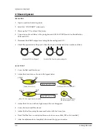
Page 48: ...o that the center of Green Red Blue pattern is aligned on the center of screen jig 3 Enter the Convergence Mode by pressing the remote control keys in the following sequence If OSD is displayed as shown in figure below press the key to exit Then redo step 3 to enter the Convergence Mode After entering the Convergence Mode Stand by for about five seconds before doing the adjustments NOTE NOTE 4 6 C...

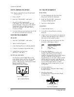
Page 49: ...Alignment and Adjustments 4 14 Samsung Electronics 4 To adjust GREEN first press the and the keys and then press the key 5 The key moves the cursor right and the key moves the cursor left ...

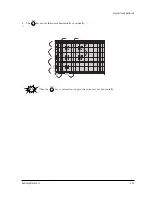
Page 50: ...Alignment and Adjustments Samsung Electronics 4 15 6 The key moves the cursor horizontally or vertically NOTE When the key is pressed once again the cursor moves horizontally ...

Page 51: ...alance 8 After the Line Shift is cancelled by pressing the key use the Channel and Volume keys Up Down to make big adjustments 9 After the green convergence adjustments are completed press the key to save the data The minor adjustments can be done only when adjusting Red and Blue ...

Page 52: ...onics 4 17 10 Superimpose the Red and Green colors by pressing the and the keys 11 To adjust RED redo steps 5 8 12 Use the key to make minor adjustments Or the key can be used for minor adjustment Cursor Movement when making minor adjustments ...

Page 53: ...the key for R Mute 2 the key to cancel the B Mute and 3 the key for B select 14 To adjust BLUE redo steps 5 8 12 15 If any color is not properly adjusted when displaying the red blue and green colors readjust the color When readjusting a color enter the minor adjustment mode Otherwise the existing adjustment data might be distorted NOTE ...

Page 54: ...16 After the color adjustments are completed press the key to save the data The cursor moves to center and then automatically moves up and to the left about five seconds later 17 After the Convergence Adjustments are completed press the key to exit NOTE ...

Page 55: ... U H POS LEFT RIGHT H SCALE SHRINK GROW V POS DOWN UP V SCALE SHRINK GROW RECALL SETTINGS EXIT SAVE AND E XI T SETUP MENU T V SE T UP COMPUTER SETUP PICTURE SETUP EXIT TV SETUP MENU V SCAL E SHRI N K GROW PC Enter PC Enter Switch to External Mode TV External Key Switch to PC Mode Select Key Select menu F Menu Key Select TV Setup CH Down key Select TV Setup Volume key Adjust horizontal position lef...

Page 56: ...ND EXIT PICTURE SETUP MENU F L I CKE R F I L T E R PI CTURE SETUP MENU BRIGHTNESS COLOR SATURETION FLICKER FILTER VIDEO FILTER RECALL SETTINGS EXIT SAVE AND E XI T SETUP MENU TV SETUP COMPUTER SETUP P I CT URE SE T UP EXIT P C MAIN MENU ZOOM COMPRESS FREEZE SE T UP RESET EXIT Select Picture Setup CH Down key Select Picture Setup Volume key Set in the bright screen Adjust brightness Volume key Set ...

Page 57: ...GHT H SCALE SHRINK GROW V P OS DOW N UP V SCALE SHRINK GROW RECALL SETTINGS EXIT SAVE AND EXIT COMPUTER SETUP MENU H POS LEFT RIGHT H SCALE SHRINK GROW V POS DOWN UP V SCALE SHRINK GROW RECALL SETTINGS EXIT SAVE AND E XI T SETUP MENU TV SETUP COMPUT E R SE T UP PICTURE SETUP EXIT COMPUTER SETUP MENU V SCAL E SHRI N K GROW Select Computer Setup CH Down key Select Computer Setup Volume key Adjust sc...

Page 58: ... SUB AFT KEY1 MAIN AFT KEY2 KEY3 ANALOG GND HALF TONE OSD B ANALOG VCC OSD G OSD R D2 POWER2 BUS STOP HOLD SCL 3 SDA 3 TIMER LED S W MUTE D1 AMP MUTE 3D RESET N C XTAL GND VCC GND XTAL2 XTAL1 RESET N C N C D3 SCL 1 SDA 1 VSYNC HSYNC BLANK 1 2 3 4 5 6 7 8 9 10 11 12 13 14 15 16 17 18 19 20 21 22 23 24 25 26 52 51 50 49 48 47 46 45 44 43 42 41 40 39 38 37 36 35 34 33 32 31 30 29 28 27 Z 9 0 3 7 1 1 ...

Page 59: ...PORT 10 1H SYNC NORMAL H V SYNC 3 5V 11 SCL 2 CLOCK BUS LINE 4 5V 12 SDA 2 DATA BUS LINE 4 5V 13 CVBS CVBS 1 7V 14 LOOP FILTER LOOP FILTER 1 9V 15 ANALOG GND GND GND 16 SUB AFT SUB AUTO FINE TURNING CONTROL 2 64V 17 KEY 1 KEY SCAN 1 4 84V 18 MAIN AFT MAIN TUNER AFT 1 9V 19 KEY 2 KEY SCAN 2 20 KEY 3 KEY SCAN 3 21 ANALOG GND GND 22 ANALOG VCC VCC 5V 23 HALF TONE SIGNAL FOR OSC FREQUENCY OSD CONTROL ...

Page 60: ... 35 RESET RESET 4 74V 36 XTAL1 XTAL 1 1 72V 37 XTAL2 XTAL 2 2 2V 38 GND GND 39 VCC VCC 5V 40 XTAL GND GND 41 N C N C 42 3D RESET 3D PHONIC RESET 5V 43 AMP MUTE MAIN AMP MUTE 44 D1 CONVERGENCE D1 45 S W MUTE SWITCH MUTE NOT USED 46 TIMER LED TIMER LED 4 7V 47 SDA 3 DATA BUS LINE 4 6V 48 SCL 3 CLOCK BUS LINE 4 6V 49 HOLD HOLD 4 65V 50 BUS STOP I2 C BUS STOP 5V 51 POWER2 PC POWER CONTROL 4 65V 52 D2 ...

Page 61: ...0 GND GND GND 11 HS1 1H SYNC OUT 12 VS1 VS1 OUT 13 GND GND GND 14 SDA 2 SERIAL DATA LINE 2 4 7V 15 SCL 2 SERIAL CLOCK LINE 2 4 8V 16 5V 5V 5V 17 HD H DRIVE OUT 1 6V 18 H BLK H BLANK INPUT 19 VD VERTICAL DRIVE VOLTAGE 2 90V 20 VD VERTICAL DRIVE VOLTAGE 2 95V 21 ABL ABL INPUT 2 15V 22 V BLK V BLANKING 23 EW EAST WEST OUT 2 2V 24 N C N C 25 GND GND GND 26 V OUT V OUT N C 27 H OUT H OUT N C 28 HC 5V I...

Page 62: ...D B INPUT 40 YS BLANK MICOM OUT 41 YM HALF TONE INPUT 42 V MUTE VIDEO MUTE V CHIP ON 4 72V 43 GND GND GND 44 9V 9V 9V 45 D Pr D Pr INPUT 46 D Y D Y INPUT 47 D Pb D Pb INPUT 48 PIP F B N C 49 GND GND GND 50 R OUT R OUT 51 G OUT G OUT 52 B OUT B OUT 53 GND GND GND 54 IK IK OUT 3 65V 55 SPOT SPOT OUT 56 GND GND GND 57 VM Y VM Y OUT 5 42V 58 VM MUTE N C PIN NO ITEM FUNCTION OUT VOLT ...

Page 63: ... 2 02V 8 PIP Y G PIP Y G DVD SIG OUT 2 04V 9 PIP Pb B PIP Pb B DVD SIG OUT 2 02V 10 PIP FB PIP FAST BLANKING 2 02V 11 12V 12V INPUT 12V 12 PIP F B N C N C 13 PIP B DVD B IN 14 PIP G DVD G IN 15 PIP R DVD R IN 16 N C N C 17 V SYNC V SYNC INPUT 18 H SYNC H SYNC INPUT 19 SCL SERIAL CLOCK LINE 4 11V 20 SDA SERIAL DATA LINE 4 5V 21 5V 5V INPUT 5V 22 GND GND GND PIN NO ITEM FUNCTION OUT VOLT ...

Page 64: ...RIAL DATA LINE 4 1V 7 V 3D COPY GUARD REJECT SIGNAL 3 8V 8 5V 5V INPUT 5V 9 Y OUT MAIN Y OUT 10 GND GND GND 11 C OUT MAIN C OUT 12 GND GND GND 1 SIF SIF OUT 3 25V 2 9V 9V INPUT 9V 3 GND GND GND 4 IF IF INPUT 4 5V 5 GND GND GND 6 AGC RF AGC IN 5 37V 7 TV VIDEO TV VIDEO OUT 8 AFT MAIN AFT INPUT 2V 9 GND GND GND PIN NO ITEM FUNCTION OUT VOLT PIN NO ITEM FUNCTION OUT VOLT 4 8 6 IF MODULE ...

Page 65: ...R IN PC R INPUT 4 G IN PC G INPUT 5 B IN PC B INPUT 6 GND GND GND 7 HS PC H SYNC INPUT 8 VS PC V SYNC INPUT 9 GND GND GND 10 SDA SERIAL DATA LINE 11 SCL SERIAL CLOCK LINE 12 GND GND GND 13 IR INPUT REMOCON 2 5V 14 GND GND GND 15 R OUT Y3 PC Y3 OUT 16 N C N C 17 B OUT C3 PC C3 OUT PIN NO ITEM FUNCTION OUT VOLT ...

Page 66: ...12V INPUT 12V 10 ENABLE 3D ENABLE 5V 11 RESET 3D RESET 5V 12 SDA SERIAL DATA LINE 4 96V 13 SCL SERIAL CLOCK LINE 4 96V 14 5V 5V INPUT 5V 15 L IN 3D L INPUT 3 86V 16 GND GND GND 17 R IN 3D R INPUT 3 22V 1 TV R TV R SOUND OUT 2 TV L TV L SOUND OUT 3 SCL SERIAL CLOCK LINE 4 SDA SERIAL DATA LINE 5 N C N C 6 GND GND GND 7 SIF SIF INPUT 8 N C N C 9 N C N C 10 9V 9V INPUT 9V PIN NO ITEM FUNCTION OUT VOLT...

Page 67: ...IV H 8 FBT DC FBT DC FEED BACK 4 87V 9 X RAY X RAY PROTECT F B 2 10V 10 N C N C 11 HV REG HV REG 3 54V 12 HV DRIVE HIGH VOLTAGE DRIVE 0 32V 13 H DRIVE H DRIVE OUT 25V 14 GND GND GND 15 HEATER HEATER INPUT AC 0 7V 16 N C N C 17 208V 208V INPUT 208V 18 N C N C 19 GND GND GND 20 V2 V2 INPUT 21 N C N C 22 N C N C 23 D FOCUS DYNAMIC FOCUS OUT 24 N C N C 25 N C N C 26 SCREEN SCREEN INPUT 1356V PIN NO IT...

Page 68: ... 8 RV RED VERTICAL OUT 9 RH RED HORIZONTAL OUT 10 5 4V 5 4V INPUT 5 4V 11 5 4V 5 4V INPUT 5 4V 12 V BLK V BLK INPUT 13 GND GND GND 14 H BLK H BLK INPUT 0 52V 15 COMP COMP VIDEO OUTPUT N C N C 16 IR INPUT REMOCON 3V 17 CTRL CTRL N C N C 18 D3 SEL D3 0 2V 19 B WHEN TEST PATTERN B OUT 20 G TEST WHEN TEST PATTERN G OUT 21 R WHEN TEST PATTERN R OUT 22 SYNC SYNC OUTPUT 4 41V PIN NO ITEM FUNCTION OUT VOL...

Page 69: ...MEMO 4 34 Samsung Electronics ...

Page 70: ...mal Abnormal Check the output voltage and waveform of CN802 CN203 on the Convergence Board Check HZ01 out pin BV BH RV RH GV GH Check the associated circuitry Check Convergence Module 1 Check F802 F855 F805 F806 on the SUB Board 2 Check the output from H BLK V BLK D1 D2 D3 on the Main Board Normal ...

Page 71: ... 5 Abnormal Check F854 on the SUB Board Normal Check IC665 output pins 7 11 Abnormal Check the mute circuit Normal Check IC601 input pins 35 38 Check IC665 Abnormal Check H006 input pins 15 17 Normal Check the 3D Phonic circuit Abnormal Check ICV01 Input pins 49 51 Normal Check ICV01 Abnormal Abnormal Insert CN601 Connector Abnormal Check H003 out Pins 1 2 Normal Normal Check Tone Control ...

Page 72: ...l Check H007 Normal Check H007 input pins 3 4 Check ICV01 Abnormal Check ICV01 input pin 48 Normal Check H009 Abnormal Check H009 input pin 1 Normal Check ICV01 Abnormal Abnormal Abnormal Check H004 Check CRT PCB pin 1 Normal Check ICV01 input pin 50 Abnormal Normal Check CN402 input pin 12 HV DRIVER Check H401 CN402 HV REG Normal Check H401 OUT BLOCK Abnormal Check H401 IC471 Abnormal Abnormal Ch...

Page 73: ...MEMO 5 4 Samsung Electronics ...

Page 74: ... BLK L740 1 AA67 00052A MIRROR FRONT 65W GLASS T3 0 FSM 1210 1 AA63 00242A COVER DUST 65W2DR WOOD BLK 1 AA63 00109A COVER MIRROR HCJ655W WOOD BLK 1 AA63 00236A COVER BACK TOP 65W2DR WOOD BLK 1 AA64 00623A CABINET BACK BOARD 652W HARDBOARD HIPS 1 AA95 00157E ASSY PCB CONVERGENCE HCJ652W SVP 65W2D 1 AA95 00325A ASSY PCB SUB HCJ652WX XAA P51A USA 1 AA94 01247B ASSY PCB MAIN OPT HCJ652WX XAA P51A USA ...

Page 75: ...0 C AL 100uF 20 50V GP TP 8x11 5 5 C552 2201 000119 C CERAMIC DISC 100nF 80 20 50V Y5V TP C639 2401 002009 C AL 100uF 20 16V GP TP 6 3x7 5 C640 2201 000119 C CERAMIC DISC 100nF 80 20 50V Y5V TP C664 2401 001068 C AL 3300uF 20 50V GP BK 22x40 10 C665 2401 000737 C AL 2200uF 20 50V GP TP 18x35 5 7 5 C666 2305 000665 C FILM MPEF 100nF 5 63V TP 7 5x4 0x5 0m C667 2401 000603 C AL 1uF 20 50V GP TP 5x11 ...

Page 76: ...165 IC POSI ADJUST REG 78R12 TO 220 3P H SINK IC502 1203 000203 IC POSI ADJUST REG 3050 TO 220 5P PLA H SINK IC503 1203 000203 IC POSI ADJUST REG 3050 TO 220 5P PLA H SINK IC504 1203 000203 IC POSI ADJUST REG 3050 TO 220 5P PLA H SINK IC506 1203 000293 IC POSI FIXED REG 7808 TO 220 3P PLAS IC507 1204 001510 IC SEPARATOR EL4583CN DIP 16P PLASTIC IC665 1201 001026 IC POWER AMP 7265 ZIP 11P 19 6MIL D...

Page 77: ...HM 5 1 8W AA TP 1 8X3 2MM R907 2001 000429 R CARBON 1KOHM 5 1 8W AA TP 1 8X3 2MM R908 2001 000515 R CARBON 220OHM 5 1 8W AA TP 1 8X3 2MM R909 2001 000515 R CARBON 220OHM 5 1 8W AA TP 1 8X3 2MM R910 2001 000515 R CARBON 220OHM 5 1 8W AA TP 1 8X3 2MM R912 2001 000003 R CARBON 330ohm 5 1 8W AA TP 1 8x3 2mm R913 2001 000786 R CARBON 47KOHM 5 1 8W AA TP 1 8X3 2MM R914 2001 000281 R CARBON 100OHM 5 1 8W...

Page 78: ...10051ASCREW WOOD PH M4 L16 ZPC BLK SWRCH18A CABW AA64 00437ACABINET WOOD HCJ652W WOOD BLK CABWOO AA60 10050XSCREW WOOD FH M3 5 L32 ZPC YEL SWRCH1 CAL 2401 003494 C AL 2 7uF 10 100V BP BK 10x13mm 5 CAS CW AA60 10051ASCREW WOOD PH M4 L16 ZPC BLK SWRCH18A CASTER AA61 00030ACASTER SVP 614JM POLYURETHANE 50 23 C SPK 3001 001045 SPEAKER 15W 8ohm 91dB 65Hz C WIRE AA39 20609ALEAD CONNECTOR ASSY SMH250 02 ...

Page 79: ...872 R CHIP 4 7KOHM 5 1 10W DA TP 2012 RP30 2007 000872 R CHIP 4 7KOHM 5 1 10W DA TP 2012 RP31 2007 001071 R CHIP 6 8KOHM 5 1 10W DA TP 2012 RP32 2007 000642 R CHIP 270OHM 5 1 10W DA TP 2012 RP33 2007 000401 R CHIP 150OHM 5 1 10W DA TP 2012 RP34 2007 000872 R CHIP 4 7KOHM 5 1 10W DA TP 2012 RP35 2007 000844 R CHIP 3KOHM 5 1 10W DA TP 2012 RP36 2007 000844 R CHIP 3KOHM 5 1 10W DA TP 2012 RP37 2007 0...

Page 80: ...007 000290 R CHIP 100OHM 5 1 10W DA TP 2012 RF12 2007 000401 R CHIP 150OHM 5 1 10W DA TP 2012 RF13 2007 000290 R CHIP 100OHM 5 1 10W DA TP 2012 RF14 2007 000401 R CHIP 150OHM 5 1 10W DA TP 2012 RF15 2007 000290 R CHIP 100OHM 5 1 10W DA TP 2012 RF16 2007 000477 R CHIP 1MOHM 5 1 10W DA TP 2012 RF17 2007 000477 R CHIP 1MOHM 5 1 10W DA TP 2012 RF18 2007 000872 R CHIP 4 7KOHM 5 1 10W DA TP 2012 RF19 20...

Page 81: ... 33uH 5 2 5x3 4mm LD04 2701 000180 INDUCTOR AXIAL 33uH 5 2 5x3 4mm LD05 2701 000136 INDUCTOR AXIAL 18uH 10 2 5x3 4mm LD06 2701 000136 INDUCTOR AXIAL 18uH 10 2 5x3 4mm LD07 2901 000297 FILTER EMI ON BOARD 3A 3 5x5 TP LD08 2701 000136 INDUCTOR AXIAL 18uH 10 2 5x3 4mm PCB AA41 10956BPCB 3D COMB P51A 2L FR 4 180X245X1 6T 6A QD09 0501 000344 TR SMALL SIGNAL KSC1623 G NPN 200mW SOT QD10 0501 000344 TR S...

Page 82: ... C818 2301 001216 C FILM PPF 47nF 5 630V TP 20x14 5x22 7 C831 2306 000323 C FILM MPPF 2 2nF 5 1 6KV TP 28 5x15 5x C833 2201 000292 C CERAMIC DISC 1nF 10 50V Y5P TP 5x3 5 C834 2401 003028 C AL 100uF 20 25V WT TP 6 3x11 5 C835 2401 000030 C AL 22uF 20 25V GP TP 5x11 5 C842 2401 003370 C AL 47uF 20 450V GP BK 16X35 5 7 C851 2201 000551 C CERAMIC DISC 0 47nF 10 1kV Y5P TP 6 3 C852 2401 000133 C AL 100...

Page 83: ...N 430OHM 5 1 8W AA TP 1 8X3 2MM R314 2001 000761 R CARBON 430OHM 5 1 8W AA TP 1 8X3 2MM R332 2001 001107 R CARBON S 220ohm 5 1 2W AA TP 2 4x6 4 R333 2001 001107 R CARBON S 220ohm 5 1 2W AA TP 2 4x6 4 R334 2001 001107 R CARBON S 220ohm 5 1 2W AA TP 2 4x6 4 R405 2009 001109 R TEMPERATURE 240ohm 5 1 4W AA TP 2 3x6 R406 2004 001983 R METAL S 2 49Kohm 1 1 2W AA TP 2 4x6 R407 2004 001897 R METAL S 43 2K...

Page 84: ... 000471 C AL 10uF 20 50V BP TP 5x11 5mm CD169 2401 000480 C AL 10uF 20 50V GP TP 5x11 5 CD170 2401 000027 C AL 4 7uF 20 50V GP TP 5x11 5 CD171 2401 000027 C AL 4 7uF 20 50V GP TP 5x11 5 CD172 2401 000480 C AL 10uF 20 50V GP TP 5x11 5 CD173 2401 000471 C AL 10uF 20 50V BP TP 5x11 5mm CD174 2401 000480 C AL 10uF 20 50V GP TP 5x11 5 CD175 2401 000480 C AL 10uF 20 50V GP TP 5x11 5 CD176 2401 000027 C ...

Page 85: ...301 000383 C FILM PEF 10nF 5 50V TP 6x7x3 2mm 5mm CY02 2401 001537 C AL 47uF 20 25V GP TP 6 3x7mm 5mm CY03 2306 000122 C FILM MPPF 100nF 5 50V TP 7 3x4 0x5 0m CY04 2401 000444 C AL 10uF 20 25V GP TP 5x5mm 5mm CY05 2401 000486 C AL 10uF 20 50V GP TP 6 3x7mm 5 CY06 2306 000122 C FILM MPPF 100nF 5 50V TP 7 3x4 0x5 0m DAL AA64 50253ADOOR AL SVP 555JHD T1 0 AL TITAN DB BM 6006 000255 SCREW ASS Y MACH W...

Page 86: ... V2 NTR 25MM ALL MODE CNT01 3711 003630 CONNECTOR HEADER BOX 32P 2R 2 54mm ANGLE CNT02 3711 003630 CONNECTOR HEADER BOX 32P 2R 2 54mm ANGLE CNY02 3711 003601 CONNECTOR HEADER BOX 12P 1R 2 5mm ANGLE CNY03 AA39 20052DLEAD CONNECTOR ASSY YBNH025 04 YSH025 CORE 3301 001201 CORE FERRITE AE 230 5x10 25x36mm 1500 28 CV01 2401 002009 C AL 100uF 20 16V GP TP 6 3x7 5 CV02 2201 000982 C CERAMIC DISC 10nF 80 ...

Page 87: ...AA TP 2 4X6 4M RV06 2001 001050 R CARBON S 1 5KOHM 5 1 2W AA TP 2 4X6 RV07 2001 000019 R CARBON S 10OHM 5 1 2W AA TP 2 4X6 4M RV08 2001 001187 R CARBON S 75OHM 5 1 2W AA TP 2 4X6 4M RV09 2001 000085 R CARBON S 100KOHM 5 1 2W AA TP 2 4X6 RV10 2001 000085 R CARBON S 100KOHM 5 1 2W AA TP 2 4X6 RV11 2001 000019 R CARBON S 10OHM 5 1 2W AA TP 2 4X6 4M RV12 2001 001187 R CARBON S 75OHM 5 1 2W AA TP 2 4X6...

Page 88: ...1 5nF 10 50V X7R TP 2012 C295 2203 000239 C CERAMIC CHIP 0 1nF 5 50V NP0 TP 2012 C296 2203 000218 C CERAMIC CHIP 100nF 20 50V Y5V TP 2012 C297 2203 000218 C CERAMIC CHIP 100nF 20 50V Y5V TP 2012 C298 2203 000218 C CERAMIC CHIP 100nF 20 50V Y5V TP 2012 C299 2203 000218 C CERAMIC CHIP 100nF 20 50V Y5V TP 2012 C401 2203 000925 C CERAMIC CHIP 470NF 80 20 50V Y5V TP C402 2203 000218 C CERAMIC CHIP 100n...

Page 89: ...QY20 0501 000344 TR SMALL SIGNAL KSC1623 G NPN 200mW SOT QY21 0501 000280 TR SMALL SIGNAL KSA1182 PNP 150mW SOT 23 R1 2007 000947 R CHIP 47OHM 5 1 10W DA TP 2012 R11 2007 000947 R CHIP 47OHM 5 1 10W DA TP 2012 R13 2007 000947 R CHIP 47OHM 5 1 10W DA TP 2012 R15 2007 000947 R CHIP 47OHM 5 1 10W DA TP 2012 R16 2007 000947 R CHIP 47OHM 5 1 10W DA TP 2012 R18 2007 000947 R CHIP 47OHM 5 1 10W DA TP 201...

Page 90: ...2007 000653 R CHIP 27KOHM 5 1 10W DA TP 2012 RY68 2007 001092 R CHIP 620OHM 5 1 10W DA TP 2012 RY70 2007 000468 R CHIP 1KOHM 5 1 10W DA TP 2012 RY71 2001 000429 R CARBON 1KOHM 5 1 8W AA TP 1 8X3 2MM RY72 2001 000429 R CARBON 1KOHM 5 1 8W AA TP 1 8X3 2MM RY73 2007 001201 R CHIP 820OHM 5 1 10W DA TP 2012 RY74 2007 000290 R CHIP 100OHM 5 1 10W DA TP 2012 RY75 2007 000290 R CHIP 100OHM 5 1 10W DA TP 2...

Page 91: ... 0402 000493 DIODE RECTIFIER 1R5GU41 400V 1 5A DO 15L D504 0401 000005 DIODE SWITCHING 1N4148 100V 200MA DO 35 D531 0402 000546 DIODE RECTIFIER TVR10G 400V 1 0A DO 41 T D532 0402 000546 DIODE RECTIFIER TVR10G 400V 1 0A DO 41 T D533 0402 000493 DIODE RECTIFIER 1R5GU41 400V 1 5A DO 15L D561 0402 000546 DIODE RECTIFIER TVR10G 400V 1 0A DO 41 T D562 0402 000546 DIODE RECTIFIER TVR10G 400V 1 0A DO 41 T...

Page 92: ...CHIP 10nF 10 50V X7R TP 2012 C137 2203 000260 C CERAMIC CHIP 10nF 10 50V X7R TP 2012 C138 2404 000275 C TA CHIP 100UF 10 10V GP TP 7343 C139 2404 000275 C TA CHIP 100UF 10 10V GP TP 7343 C140 2203 000260 C CERAMIC CHIP 10nF 10 50V X7R TP 2012 C141 2203 000260 C CERAMIC CHIP 10nF 10 50V X7R TP 2012 C142 2404 000275 C TA CHIP 100UF 10 10V GP TP 7343 C143 2404 000123 C TA CHIP 10uF 20 16V TP 6032 2 9...

Page 93: ...0342 TR SMALL SIGNAL KSC1623 Y NPN 200mW SOT Q104 0501 000342 TR SMALL SIGNAL KSC1623 Y NPN 200mW SOT Q105 0501 000342 TR SMALL SIGNAL KSC1623 Y NPN 200mW SOT Q106 0501 000342 TR SMALL SIGNAL KSC1623 Y NPN 200mW SOT Q107 0501 000342 TR SMALL SIGNAL KSC1623 Y NPN 200mW SOT Q108 0501 000342 TR SMALL SIGNAL KSC1623 Y NPN 200mW SOT Q109 0501 000342 TR SMALL SIGNAL KSC1623 Y NPN 200mW SOT Q110 0501 000...

Page 94: ...07 000300 R CHIP 10KOHM 5 1 10W DA TP 2012 R244 2007 001039 R CHIP 56KOHM 5 1 10W DA TP 2012 R245 2007 000030 R CHIP 560OHM 5 1 10W DA TP 2012 R246 2007 000300 R CHIP 10KOHM 5 1 10W DA TP 2012 R247 2007 001039 R CHIP 56KOHM 5 1 10W DA TP 2012 R248 2007 000030 R CHIP 560OHM 5 1 10W DA TP 2012 R249 2007 000300 R CHIP 10KOHM 5 1 10W DA TP 2012 R250 2007 001039 R CHIP 56KOHM 5 1 10W DA TP 2012 R251 20...

Page 95: ... 00135BPCB CONVERGENCE P51A 1L CEM 1 330x245x1 R382 2002 001006 R COMPOSITION 4 7Kohm 5 1 2W AA TP 3 7x R476 2004 004046 R METAL S 430Kohm 1 1 2W AA TP 2 5x6 5 R476A 2004 004001 R METAL S 180Kohm 1 1 2W AA TP 2 5x6 5 R476B 2004 001892 R METAL S 162Kohm 1 1 2W AA TP 2 5x6 5 R476C 2004 004046 R METAL S 430Kohm 1 1 2W AA TP 2 5x6 5 R478 2004 001892 R METAL S 162Kohm 1 1 2W AA TP 2 5x6 5 R501 2004 001...

Page 96: ...F 5 63V TP 5mm C361 2306 000122 C FILM MPPF 100nF 5 50V TP 7 3x4 0x5 0m C362 2305 000149 C FILM MPEF 100nF 5 100V TP 12x12 5x6 5 C371 2401 000302 C AL 100uF 20 25V GP TP 6 3x11 5 C372 2401 000480 C AL 10uF 20 50V GP TP 5x11 5 C373 2401 000302 C AL 100uF 20 25V GP TP 6 3x11 5 C374 2401 001621 C AL 6 8uF 20 450V GP TP 13x20 5 C405 2201 000558 C CERAMIC DISC 0 47nF 10 50V Y5P TP 5x3 C406 2201 000370 ...

Page 97: ...3 2MM R387 2001 000009 R CARBON 20KOHM 5 1 8W AA TP 1 8X3 2MM R388 2001 000522 R CARBON 22KOHM 5 1 8W AA TP 1 8X3 2MM R389 2001 000577 R CARBON 2KOHM 5 1 8W AA TP 1 8X3 2MM R395 2001 000734 R CARBON 4 7KOHM 5 1 8W AA TP 1 8X3 2M R397 2001 000429 R CARBON 1KOHM 5 1 8W AA TP 1 8X3 2MM R411 2001 000734 R CARBON 4 7KOHM 5 1 8W AA TP 1 8X3 2M R412 2001 001088 R CARBON S 1KOHM 5 1 2W AA TP 2 4X6 4M R413...

Page 98: ...2 4x6 4mm RC604 2004 001390 R METAL S 1Kohm 2 1 2W AA TP 2 4x6 4mm RC605 2001 001093 R CARBON S 2 2KOHM 5 1 2W AA TP 2 4X6 RC606 2001 001103 R CARBON S 20KOHM 5 1 2W AA TP 2 4X6 4 RC607 2001 001146 R CARBON S 4 7OHM 5 1 2W AA TP 2 4X6 4 RC608 2001 001131 R CARBON S 33KOHM 5 1 2W AA TP 2 4X6 4 RC611 2001 001108 R CARBON S 22KOHM 5 1 2W AA TP 2 4X6 4 RC612 2001 001067 R CARBON S 11KOHM 5 1 2W AA TP ...

Page 99: ...L R IN SC SL SR OUT PCS L R IN Y Pb Pr IN EEPROM Korea MK201 USA TDA9850 D Sub 15Pin R G B H V CRT Block R G B Drive TDA6110Q FROM MAIN R Drive TDA6111Q G Drive TDA6111Q B Drive TDA6111Q SDA2 SCL2 REAR S Video Y1 C1 MAIN CVBS Yin1 Cin1 MTV L R STV L R Y3 C3 MTV V STV V SIF RF RF Encoder F C FS310KBC 3D COMB U p d6488 U p c1862gs 2T PIP TDA9160A SUB CVBS MAIN CVBS CAP CL DA ENA S c a n C o n v e r ...

Page 100: ... S W Yin 1 C in 1 MAI N CVB S R F Su b R F Main SDA1 SCL1 SDA3 SCL3 SDA4 SCL4 Y3 C3 S Ja ck S W V2 S W Y1 C1 V2 V2 S W V1 MTV STV Y1 C 1 S W V2 S W Y1 C1 V2 R G B H V E P r E P b E Y REAR Side Side 8 3 Sound SIGNAL A V Switching TA8851 L R 7 6 EA L R 3 1 EA L 1 R 1 IN L 2 R 2 IN ML MR O U T YU V L R IN Y P b P r IN P C S L R IN SC S L S R O U T MT S Main L R R F Su b L R 3 D P h o n ic T MS 57052 ...

Page 101: ...D BY RECTIFIER RBV 606 S W IC STR F6656 TRANS EER 5345 PC PS2561 ERROR AMP SE110N 117V 1 0A 8 5V 0 8A 8 5V 0 5A 34 0V 1 2A 30V 0 7A 13 5V 1 2A 30V 0 7A STAND BY LINE FILTER 1mH 5A FUSE LINE FILTER 1mH 5A RELAY POWER ON OFF RELAY SWITCHING CONTROLLER AC IN P UT H O T C O L D POWER ...

Page 102: ...8 4 Samsung Electronics MEMO ...

Page 103: ...G N D M A I N Y G N D M A I N C G N D Y U b V r G N D D P r D Y D P b G N D P C B P C G C N T 0 1 C N T 0 2 S C2 NC S2 DE T S Y 2 GND R3 NC GND L 3 NC V3 DE T V3 SIDE A V S C2 NC S2 DE T S Y 2 GND R3 NC GND L 3 NC V3 DE T V3 12P C N Y 0 2 K E Y 2 K E Y 1 S T D 5 V G N D K E Y 3 I R T I M E R L E D 1 3 5 V S D A 1 S C L 1 G N D 8P K E Y 2 K E Y 1 S T D 5 V G N D K E Y 3 I R T I M E R L E D 1 3 5 V ...

Page 104: ...10 Schematic Diagrams 10 1 MAIN A Schematic Diagrams Samsung Electronics 10 1 TP01 TP02 182 P SCL 2 SDA 2 Power Line Signal Line TP01 TP02 ...

Page 105: ...Schematic Diagrams 10 2 Samsung Electronics 10 2 MAIN B TP09 TP08 TP07 TP06 TP05 TP04 TP03 TP02 TP01 12 TP01 TP02 TP03 TP04 TP05 TP06 TP07 TP08 TP09 Power Line Signal Line ...

Page 106: ...Schematic Diagrams Samsung Electronics 10 3 10 3 MAIN C TP02 TP03 TP01 TP04 Power Line Signal Line TP01 TP02 TP03 TP04 ...

Page 107: ...Schematic Diagrams 10 4 Samsung Electronics 10 4 MAIN D TP01 TP02 TP03 Power Line Signal Line TP01 TP02 TP03 ...

Page 108: ...Schematic Diagrams Samsung Electronics 10 5 10 5 SUB POWER DEFL 1 TP01 TP04 TP02 TP03 TP05 TP06 TP07 TP09 TP08 TP01 TP02 TP03 TP04 TP05 TP06 TP07 TP08 TP09 Power Line Signal Line ...

Page 109: ...Schematic Diagrams 10 6 Samsung Electronics 10 6 SUB POWER DEFL 2 TP01 Power Line Signal Line TP01 ...

Page 110: ...Schematic Diagrams Samsung Electronics 10 7 10 7 CRT ...

Page 111: ...Schematic Diagrams 10 8 Samsung Electronics 10 8 CONVERGENCE TP01 TP02 TP03 TP04 TP05 TP06 Power Line Signal Line TP01 TP02 TP03 TP04 TP05 TP06 ...

Page 112: ...Schematic Diagrams Samsung Electronics 10 9 10 9 CONVERGENCE MOL ...

Page 113: ...Schematic Diagrams 10 10 Samsung Electronics 10 10 HV MODULE TP01 TP02 Power Line Signal Line TP01 TP02 ...

Page 114: ...Schematic Diagrams Samsung Electronics 10 11 10 11 3D COMB 7 7 Power Line Signal Line ...

Page 115: ...Schematic Diagrams 10 12 Samsung Electronics 10 12 3D PHONIC ...

Page 116: ...Schematic Diagrams Samsung Electronics 10 13 10 13 F CONVERTER ...

Page 117: ...Schematic Diagrams 10 14 Samsung Electronics 10 14 PIP ...

Page 118: ...Schematic Diagrams Samsung Electronics 10 15 10 15 TERMINAL 1 ...

Page 119: ...Schematic Diagrams 10 16 Samsung Electronics 10 16 TERMINAL 2 ...

Page 120: ...Schematic Diagrams Samsung Electronics 10 17 10 17 IF V M MODULE ...

Page 121: ...Schematic Diagrams 10 18 Samsung Electronics 10 18 PROSCAN 1 4 Power Line Signal Line ...

Page 122: ...Schematic Diagrams Samsung Electronics 10 19 10 19 PROSCAN 2 4 Power Line Signal Line ...

Page 123: ...Schematic Diagrams 10 20 Samsung Electronics 10 20 PROSCAN 3 4 Power Line Signal Line ...

Page 124: ...Schematic Diagrams Samsung Electronics 10 21 10 21 PROSCAN 4 4 Power Line Signal Line ...

Reviews: