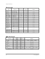


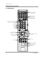


Alignment and Adjustments
4-22
Samsung Electronics
4-6 Other Adjustments
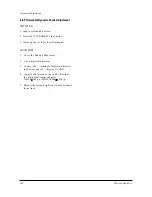
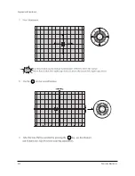
4-6-1 Screen Adjustment
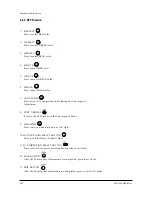
1. Warm up the TV for at least 30 minutes.
2. Turn to the Video Mode (No Signal) using a
remote-control.
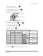
3. Connect an oscilloscope to RK,GK,BK.
4. Adjust the VR (VR501, VR531, VR561) screen
so that RK, GK, BK pulse is 20Vp-p each.
(Turn the R,G,B VR screen fully
counterclockwise in the area of each flyback
line.)
4-6-2 White Balance Adjustment
1. Select the “STANDARD” video mode.
2. Input 100% white pattern.
3. In the stand-by mode, press the remote-control
keys in the following sequence:
Displsy
→
Menu
→
Mute
→
Power ON
4. Warm up the TV for at least 30 minutes.
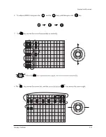
5. Input a 10-step signal.
6. R-cut off, B-cut off, and G-cut off by pressing
the /- keys.
7. Adjust the low light with viewing the dark
side of the screen.
8. Select R-drive, G-drive, and B-drive by
pressing the /- keys.
9. Adjust the high light with viewing the light
side of the screen.
10. If necessary, redo adjustments 6~9.
11. Press the Menu key to exit.
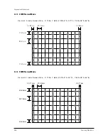
4-6-3 Sub-Brightness Adjustment
1. Input a sub-brightness adjustment signal.
(TOSHIBA PATTERN)
2. In the stand-by mode, press the remote-control
keys in the following sequence :
Displsy
→
Menu
→
Mute
→
Power ON
3. Select SBT by pressing the /- keys.
4. Adjust so that the 63 step on the right side of
the screen is not seen (Use the /-
keys).
5. Press the Menu key to exit.
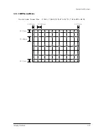
4-6-4 High Voltage (29KV) Check
PRECAUTION
1. Input a lion head pattern.
2. Select “STANDARD” video mode.
3. Warm up the TV for at least 10 minutes.
4. Use a 1000:1 probe.
ADJUSTMENT
1. Connect the (+) terminal of the 1000:1 probe to
the high voltage distributor and the (-)
terminal to GND (located on the deflection
board).
2. Adjust RR471S (located on the deflection
board) so that the digital meter indicates
DC 29V
±
0.1V.
4-6-5 F.S. (Fail Safe) Adjustment
Note : The finished product has a well-mounted
VR (RR402S).
If necessary, do the F.S. adjustments in the
following sequence.
1. Use a digital multimeter.
2. Connect the digital multimeter to the JIG pin
(DZ482S) terminals
3. Adjust VR (RR402S) so that the voltage
becomes 2.25V.
4. After the adjustments are complete, be sure to
mount VR (RR402S) correctly.
Summary of Contents for SP47W3HFX/COM
Page 2: ...ELECTRONICS Samsung Electronics Co Ltd Nov 2002 Printed in Korea 3J52A SESA 47W3 ...
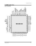
Page 11: ...Reference Information Samsung Electronics 2 5 2 3 MICOM IIC BUS LINE UP ...
Page 12: ...Reference Information 2 6 Samsung Electronics MENO ...
Page 45: ...Alignment and Adjustments Samsung Electronics 4 29 Power 4 8 2 CHINA ...
Page 49: ...Alignment and Adjustments Samsung Electronics 4 33 ...
Page 50: ...Alignment and Adjustments 4 34 Samsung Electronics ...
Page 51: ...Samsung Electronics 4 35 ...
Page 52: ...Alignment and Adjustments 4 36 Samsung Electronics ...
Page 68: ...Alignment and Adjustments 4 52 Samsung Electronics MENO ...
Page 72: ...MEMO 5 4 Samsung Electronics ...
Page 85: ...Samsung Electronics Block Diagrams 8 1 8 Block Diagram 8 1 Main Signal Progressive ...
Page 86: ...Block Diagrams 8 2 Samsung Electronics 8 2 Video Signal ...
Page 87: ...Samsung Electronics Block Diagrams 8 3 8 3 Sound Signal ...
Page 88: ...Block Diagrams 8 4 Samsung Electronics 8 4 Power Supply C ...
Page 89: ...Samsung Electronics Block Diagrams 8 5 8 5 In Out by Block 8 6 Signal Connection by Block ...
Page 90: ...Samsung Electronics Wiring Diagrams 9 1 9 1 Pcb Connection Progressive 9 Wiring Diagram ...
Page 91: ...10 Schematic Diagrams Samsung Electronics Schematic Diagrams 10 1 10 1 MAIN 1 ...
Page 92: ...Schematic Diagrams 10 2 Samsung Electronics 10 2 MAIN 2 ...
Page 93: ...Samsung Electronics Schematic Diagrams 10 3 10 3 MAIN 3 TP02 TP01 TP01 TP02 ...
Page 94: ...Schematic Diagrams 10 4 Samsung Electronics 10 4 MAIN 4 ...
Page 95: ...Samsung Electronics Schematic Diagrams 10 5 10 5 MICOM CS with out TTX TP04 TP03 TP03 TP04 ...
Page 96: ...Schematic Diagrams 10 6 Samsung Electronics 10 6 MICOM CS with in TTX TP04 TP03 TP03 TP04 ...
Page 97: ...Samsung Electronics Schematic Diagrams 10 7 10 7 MICOM CW ...
Page 98: ...Schematic Diagrams 10 8 Samsung Electronics 10 8 POWER ...
Page 99: ...Samsung Electronics Schematic Diagrams 10 9 10 9 POWER with in PFC ...
Page 100: ...Schematic Diagrams 10 10 Samsung Electronics 10 10 SOUND ...
Page 101: ...Samsung Electronics Schematic Diagrams 10 11 10 11 CRT ...
Page 104: ...Schematic Diagrams 10 14 10 13 SUB 2 TP14 TP13 TP13 TP14 ...
Page 106: ...Schematic Diagrams 10 16 Samsung Electronics 10 15 A V TERMINAL ...
Page 108: ...Schematic Diagrams 10 18 Samsung Electronics 10 17 CONVERGENCE SDC11 1 2 ...
Page 109: ...Samsung Electronics Schematic Diagrams 10 19 10 18 CONVERGENCE SDC11 2 2 ...
Page 110: ...Schematic Diagrams 10 20 Samsung Electronics 10 19 PERFECT FOCUS PHOTO SENSOR INTERFACE BOARD ...
Page 111: ...Samsung Electronics Schematic Diagrams 10 21 10 20 AV FRONT ...
Page 112: ...Schematic Diagrams 10 22 Samsung Electronics 10 21 CONTROL VM CONTROL VM ...
Page 113: ...Samsung Electronics Schematic Diagrams 10 23 10 22 DW 1 ...
Page 114: ...Schematic Diagrams 10 24 Samsung Electronics 10 23 DW 2 ...
Page 117: ...Samsung Electronics Schematic Diagrams 10 27 10 25 SUB AMP PFC SUB AMP PFC ...
Page 118: ...Schematic Diagrams 10 28 Samsung Electronics 10 26 FORMAT CONVERTER ...


