Samsung SGH-Z630, Service Manual
The Samsung SGH-Z630 Service Manual is a comprehensive guide for users seeking detailed information about their device's features and functions. This manual is available for free download on our website, providing users with valuable insights on how to maximize the performance and troubleshoot any issues with their Samsung SGH-Z630.
Share
Download


Reviews:
No comments
Related manuals for SGH-Z630
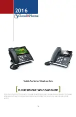
T Series
Brand: Yealink Pages: 8

G1
Brand: T-Mobile Pages: 2

W56P Telesystem
Brand: Yealink Pages: 12

Verizon One Talk W60B
Brand: Yealink Pages: 8

Telkom W52P
Brand: Yealink Pages: 2

T46S Skype for Business
Brand: Yealink Pages: 2

VP59 Teams
Brand: Yealink Pages: 533

SM-A356E
Brand: Samsung Pages: 155

HFB 400
Brand: Caliber Pages: 10

Smartphone E-11
Brand: Etisalat Pages: 75

Accessibility
Brand: Blackberry Pages: 17

IQ458
Brand: FLY Pages: 56

GXP1450
Brand: Grandstream Networks Pages: 19

Digi Walker 8870
Brand: Mio Pages: 223

V1305
Brand: Videocon Pages: 17

JA-62GSM
Brand: jablotron Pages: 11

Digital Telephones
Brand: Eon Pages: 4

Myco 2
Brand: ASCOM Pages: 112


