SGH-X100
SERVICE
Manual
GSM TELEPHONE
CONTENTS
1.
Specification
2.
Circuit Description
3.
Exploded Views and Parts List
4.
Electrical Parts List
5.
Block Diagrams
6.
PCB Diagrams
7.
Flow Chart of Troubleshooting
Page 1: ... SERVICE Manual GSM TELEPHONE CONTENTS 1 Specification 2 Circuit Description 3 Exploded Views and Parts List 4 Electrical Parts List 5 Block Diagrams 6 PCB Diagrams 7 Flow Chart of Troubleshooting GSM TELEPHONE ...
Page 2: ...nics Co Ltd June 2003 Printed in Korea Code No GH68 04326A BASIC ⓒ This Service Manual is a property of Samsung Electronics Co Ltd Any unauthorized use of Manual can be punished under applicable International and or domestic law ...
Page 3: ...805 1880 ARFCN range 1 124 0 124 975 1023 512 885 Tx Rx spacing 45MHz 45MHz 95MHz Mod Bit rate Bit Period 270 833kbps 3 692us 270 833kbps 3 692us 270 833kbps 3 692us Time Slot Period Frame Period 576 9us 4 615ms 576 9us 4 615ms 576 9us 4 615ms Modulation 0 3GMSK 0 3GMSK 0 3GMSK MS Power 33dBm 13dBm 33dBm 5dBm 30dBm 0dBm Power Class 5pcl 15pcl 5pcl 19pcl 0pcl 15pcl Sensitivity 102dBm 102dBm 100dBm ...
Page 4: ...6 31 2 dBm 7 29 2 dBm 8 27 2 dBm 9 25 2 dBm 10 23 2 dBm 11 21 2 dBm 12 19 2 dBm 13 17 2 dBm 14 15 2 dBm 15 13 2 dBm 16 11 3 dBm 17 9 3dBm 18 7 3 dBm 19 5 3 dBm TX Power control level DCS1800 0 30 3 dBm 1 28 3 dBm 2 26 3 dBm 3 24 3 dBm 4 22 3 dBm 5 20 3 dBm 6 18 3 dBm 7 16 3 dBm 8 14 3 dBm 9 12 4 dBm 10 10 4 dBm 11 8 4dBm 12 6 4 dBm 13 4 4 dBm 14 2 5 dBm 15 0 5 dBm 2 GSM TX power class ...
Page 5: ...U103 The receiver front end converts the aerial RF signal from EGSM DCS bands down to a low intermediate frequency IF of 100 kHz The first stages are symmetrical low noise amplifiers LNAs They are matched to 50 ohm The LNAs are followed by an I Q down mixer It consists of two mixers in parallel but driven by quadrature out of phase LO signals The In phase I and Quadrature phase Q IF signals are lo...
Page 6: ...grammable Pulse width modulator PWM and FET to modulate the intensity of a series of LED or to control a DC DC converter that drives LCD backlight This phone SGH X100 is not use PWM but use DC CONTROL BACKLIGHT So BACKLIGHT voltage is high value backlight is bright 1 3 Clock Generator The Clock Generator CG generates all clocks for internal and external usage The 32768 Hz crystal oscillator provid...
Page 7: ...fects Since the play data of YMU762MA3 are interpreted at anytime through FIFO the length of the data playing period is not limited so the device can flexibly support application such as incoming call melody music distribution service The hardware sequencer built in this device allows playing of the complex music without giving excessive load to the CPU of the portable telephones Moreover the regi...
Page 8: ...RAM 55 Kwords on chip program ROM in the DSP It has 4K 32bits ROM and 2K 32bits RAM in the ARM core DSP is consisted of KBS JTAG EMI and UART ARM core is consisted of EMI PIC Programmable Interrupt Controller reset power clock unit DMA controller TIC Test Interface Controller eripheral bridge PPI SSI Synchronous Serial Interface ACC Asynchronous communications controllers timer ADC RTC Real Time C...
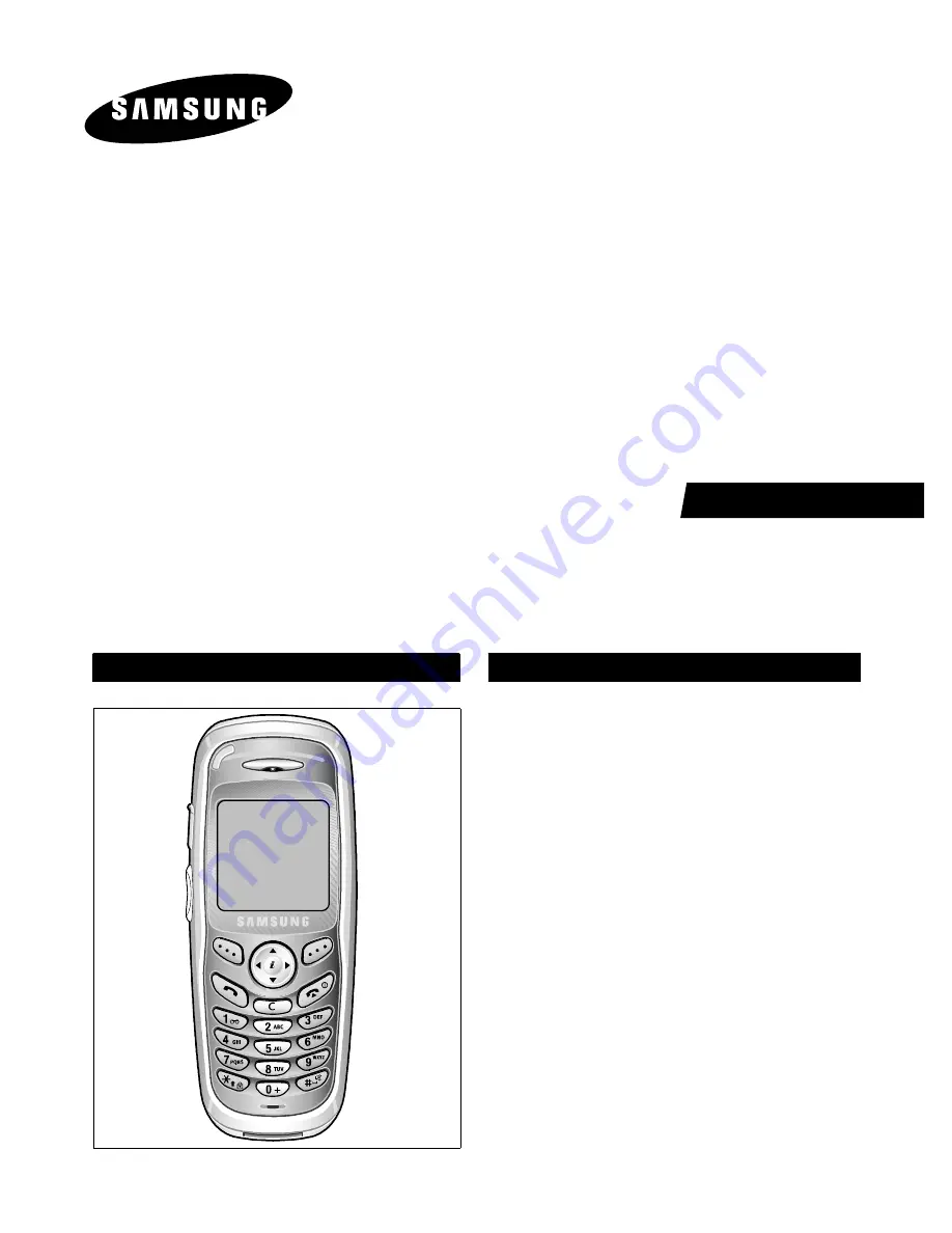
Page 9: ...ary Contents may change without notice 3 SGH X100 Exploded View and its Parts list This Document can not be used without Samsung s authorization 3 1 1 Cellular phone Exploded View 1 2 3 5 6 4 9 10 11 7 8 13 12 14 15 16 ...
Page 10: ...NO DESCRIPTION SEC CODE REMARK 1 FRONT COVER GH75 03497A 2 KEYPAD GH75 03518A 3 MOTOR GH31 00064A 4 DOME SHEET GH59 00929A 5 MIC GH30 00044A 6 IF COVER GH73 02203A 7 MICRO SPEAKER 3001 001445 8 VOLKEY GH75 03728A 9 LCD GH07 00394A 10 MAIN PBA GH92 01558A 11 SCREW 6001 001654 12 INTENNA GH42 00308A 13 REAR COVER GH75 03496A 14 RF COVER GH72 09251A 15 SCREW 6001 001654 16 BATTERY GH43 00994A ...
Page 11: ... Exploded view and its Part list This Document can not be used without Samsung s authorization 3 3 3 Test Jig GH80 01909A 3 1 RF Test Cable GH39 00140A 3 2 Test Cable GH39 00217A 3 3 Serial Cable 3 4 Power Supply Cable 3 5 DATA CABLE GH39 00219A 3 6 TA GH44 00482G ...
Page 12: ...1 001647 LED404 0601 001647 LED406 0601 001647 LED407 0601 001647 LED410 0801 002237 U300 0801 002540 U210 0801 002540 U303 0801 002540 U304 1001 001183 U212 1003 001440 Q403 1109 001280 U305 SEC CODE Design LOC 1201 001954 U101 1202 001036 U203 1203 002633 U307 1203 002980 U309 1204 002161 U301 1205 002257 U400 1205 002276 U200 1205 002327 U103 1404 001221 TH200 2909 001204 U100 1405 001082 V202 ...
Page 13: ...2 R203 2007 000162 R211 2007 000162 R212 2007 000162 R229 2007 000162 R234 2007 000162 R270 2007 000162 R300 2007 000162 R302 2007 000162 R303 2007 000162 R304 2007 000162 R306 SEC CODE Design LOC 2007 000162 R350 2007 000162 R360 2007 000162 R361 2007 000162 R436 2007 000171 R100 2007 000171 R107 2007 000171 R109 2007 000171 R139 2007 000171 R213 2007 000171 R214 2007 000171 R228 2007 000171 R307...
Page 14: ...9 R409 2007 007100 R415 2007 007107 R201 2007 007107 R209 2007 007136 R311 2007 007137 R310 2007 007137 R313 2007 007148 R104 2007 007311 R128 2007 007334 R215 2007 007480 R220 SEC CODE Design LOC 2007 007573 R428 2007 007588 R429 2007 007981 R224 2007 008312 R221 2007 008354 R427 2203 000233 C119 2203 000233 C120 2203 000233 C144 2203 000254 C145 2203 000254 C209 2203 000254 C301 2203 000254 C408...
Page 15: ...0 C139 2203 000995 C203 2203 000995 C215 2203 000995 C225 2203 000995 C226 2203 000995 C227 2203 000995 C228 2203 000995 C471 2203 001153 C146 2203 001652 C411 2203 001652 C423 SEC CODE Design LOC 2203 002443 C135 2203 003054 C220 2203 003054 C231 2203 005054 C201 2203 005054 C217 2203 005056 C222 2203 005057 C112 2203 005057 C115 2203 005057 C122 2203 005057 C134 2203 005057 C150 2203 005057 C156...
Page 16: ...2 C306 2203 005482 C309 2203 005482 C313 2203 005482 C410 2203 005482 C420 2203 005482 C470 2203 005482 C472 2203 005496 C141 2203 005496 C315 2203 005503 C138 2203 005503 C151 SEC CODE Design LOC 2203 005503 C152 2203 005503 C153 2203 005503 C154 2203 005840 C350 2203 006053 C126 2203 006053 C412 2203 006053 C424 2203 006053 C426 2203 006053 C427 2203 006053 C428 2203 006053 C429 2203 006053 C476...
Page 17: ...5 2703 001751 L121 2703 001791 L106 2703 002198 L117 2703 002201 L109 2703 002201 L111 2703 002203 L108 2703 002208 L105 2703 002208 L107 2703 002268 L116 2703 002519 L119 2801 004025 X400 2806 001317 OSC100 2809 001279 OSC101 2901 001246 U302 2901 001254 L120 2904 001417 F101 2904 001424 F102 3301 001105 L400 3404 001152 SW1 3404 001152 SW2 3705 001322 CN100 3709 001244 CN400 3710 001611 CN301 SE...
Page 18: ...dB 1805 1880 1 15 dB Atten 2xfo 39dB 30dB GSM DCS 3xfo 35dB 20dB GSM DCS EN CLK DATA DCS S W OFFSET Mixer input power 16dBm max 22dBm min fcompRF 26MHz Philips Transceiver UAA3536 Pins IA IB QA and QB VIQ 1 25Vtyp 1 15Vmin 1 35Vmax Vmod 0 5Vpp QUAD DIV PFD CP VREG Vcc_RF_LO FracN DIV 1 1 2 VREG 26MHz Vcc_REF 2 4V typ Vcc_SYN FESW1 FESW2 3 W BUS CTL REG PW R EN GSM DCS PCS DIV QUAD PFD CP fTXIF 60 ...
Page 19: ...SAMSUNG Proprietary Contents may change without notice SGH X100 Block Diagrams 5 2 This Document can not be used without Samsung s authorization 2 Base Band Solution Block Diagram ...
Page 20: ...SAMSUNG Proprietary Contents may change without notice 6 1 6 SGH X100 PCB Diagrams This Document can not be used without Samsung s authorization 1 Main PCB Top Diagram ...
Page 21: ...SAMSUNG Proprietary Contents may change without notice SGH X100 PCB Diagrams This Document can not be used without Samsung s authorization 6 2 2 Main PCB Bottom Diagram ...
Page 22: ...ry Voltage is more than 3 4V Power On does not work Change the Battery END No Yes C411 V_ISUP 2 7V Check the PMU related to V_ISUP No Yes Check the Clock at C410 32KHZ Resolder X400 No Yes C429 VDD1 H Replace the PBA No Yes C428 VDD2 C427 VDD3 2 8V Replace PBA No Yes Check for the clock at C145 13MHz Check the clock generation circuit related to OSC101 No Yes Check the initial operation ...
Page 23: ...P402 VDD_VI B C405 4 7U F VSS2 E8 VSS3 C5 VSS4 A8 VSS5 VSS6 J1 TM J3 VBAT C2 VCC B3 VIBVBA T VIBVD D A3 G6 VPRO G J4 VSAVE C3 VSS1 H4 SEL3RB C6 SIMCLK A2 SIMGND C7 SIMI O SIMSCN A1 B1 SIMSCP B2 SIMVBA T SLPMOODN D5 F5 RF2VD D H9 RF2VDDS G8 RFVBAT C1 RST RSTO N D6 E4 SCL F3 SD A E7 SEL12RB E5 REFC J6 REFGN D F8 RF1SN S E6 RF1SW S RF1VD D F9 E9 RF1VDDS H8 RF2SN S F6 RF2SW S G9 NC1 C4 NC2 F4 ONKEY_N ...
Page 24: ... Troubleshooting 7 3 This Document can not be used without Samsung s authorization 2 Initial The node between R202 and C209 H RSTON Initial Failure Check the circuit related to reset END No Yes U303 pin 4 6 memory CE is OK Yes Yes No Replace PBA Check the circuit around LCD U303 ...
Page 25: ... HA 3 N3 HA 4 K5 HA 5 M3 HA 6 P2 HA 7 HA 8 N2 J5 HA15 K3 HA16 J4 HA17 K4 HA18 K2 HA19 P3 HA 2 G4 HA20 HA21 P5 L10 GPON1 N9 GPON2 M4 HA 1 N1 HA10 L2 HA11 L1 HA12 M2 HA13 HA14 J2 GPIO1 0 L8 GPIO2 M9 GPIO3 P7 GPIO4 L7 GPIO5 L9 GPIO6 N7 GPIO7 P6 GPIO8 GPIO9 N8 CS_N1 M5 CS_N2 G3 CS_N3 B5 CTS0_N A11 EARN B10 EARP M1 2 GPIO0 K9 GPIO1 K8 D8 CD I E9 CD O D9 CEN P11 CKI P13 CKI32I P14 CKI32O N4 CS_N0 G5 G10...
Page 26: ...ed without Samsung s authorization 3 Charging Part Check the U309 pin 4 4 9 V Abnormal charging part END No Yes U309 pin 5 H No Yes Q301 pin 1 CHG_ON L No Yes Check the U309 pin 3 4 2V No Yes Check the circuit related to V_EXT_CHARGE Resolder or replace U309 Check the circuit related to CHG_ON signal Resolder or replace U309 ...
Page 27: ...SAMSUNG Proprietary Contents may change without notice SGH X100 Flow Chart of Troubleshooting This Document can not be used without Samsung s authorization 7 6 Charging ...
Page 28: ... Document can not be used without Samsung s authorization 4 Sim Part CN400 pin 1 5 H Phone can t access SIM Card Replace PBA Check the SIM Card END No Yes Yes Yes No Replace PBA After Power ON Check SIMCLK Signal on CN400 pin3 in a few second Yes No Replace PBA After SIM card insert CN400 pin 2 H SIMRST ...
Page 29: ...not be used without Samsung s authorization 7 8 5 Microphone Part Check the connection from MIC Check the circuit from U200 to MIC Resolder MIC Resolder the C200 C201 C203 C208 C210 C211 C212 C213 C215 C216 C217 R200 R204 and R206 END No Yes Yes Yes Yes No Check the MIC No Replace the MIC Microphone does not work ...
Page 30: ...0 C402 100N F C409 TP401 G 10 2 2 33 44 5 5 66 7 G G 8 9 G CN400 PC D6 A6 H2 9 S 11 TP402 4 7U F C401 C2 VCC C6 SIMCLK A2 SIMGND C7 SIMI O SIMSCN A1 B1 SIMSCP B2 SIMVBA T C1 RST IO D1 D3 CPRES D2 CLK V401 V402 C450 NC X400 SIMCLK SIMI O 100N F C212 V214 C211 56PF MIC_BIAS C217 10PF L201 27nH 10K R204 1 5K R206 V215 C201 10PF 100N F C208 C216 33PF C200 33PF 1 5K R200 C210 15PF C213 9PF 27nH L202 C2...
Page 31: ...thorization 7 10 6 Speaker Part Melody U300 pin 5 2 85V Speaker does not work Check the Clock signal at Pin 1 of U301 13MHz is OK Check the clock generation circuit related to OSC101 and U300 END No Yes No Resolder or replace U300 U301 pin 17 18 1 8V Resolder U301 Yes No Is Speaker working Check the Spearke Contact and change the Speaker Yes No ...
Page 32: ...21 D6 D7 20 EQ1 12 13 EQ2 EQ3 14 U301 YMU762 MA 3 30 A0 1 CLKI D0 27 26 D1 25 D2 C312 6 3V 4 7UF 1 2K 1 R313 3 3K R306 1 2K 1 R310 C350 1uF R304 330 NC C300 C304 VBAT 27PF VDD3 VDD3 GND 3 IN 2 NC 1 OUT 4 VCC 5 R307 TC7SH04FU TE85L U300 0 220NF C315 100NF C306 150PF C314 R350 100K Y1 _E 3 U304 1 A GND 25 VCC Y0 6 4 NC7SZ19P6X C301 10NF 27PF C308 VDD3 VDD2 C311 68NF C309 100NF 100NF C313 VDD3 4 7K 1...
Page 33: ...shooting This Document can not be used without Samsung s authorization 7 12 7 Key Data Input When one or the keys is pushed is it displayed on LCD Check the Dome sheet Key Pad END No Yes Yes Check Initial Operation When one of the keys is pushed KBIO signal is OK Replace the PBA No Yes ...
Page 34: ...ooting 7 13 This Document can not be used without Samsung s authorization 8 Receiver Part EAR201 pin 2 3 short Resolder EAR201 END No Yes Yes Receiver does not work EAR201 pin 2 3 6 1 5V Replace the PBA No Yes Is Receiver working Check the Receiver contact and Replace the Receiver No Yes ...
Page 35: ...on 7 14 9 Back Light for Color Main LCD LCD Contrast high level in the Menu Select LCD Contrast high level END No Yes Yes Backlight does not work U307 pin 5 3 35 Resolder U307 No Yes U307 pin 4 H Replace the PBA No Yes U307 pin 1 10V Check U307 and L300 No Yes Yes Backlight does work Check D600 ZD600 and resolder LCD Module Or replace the LCD Module No ...
Page 36: ...e without notice SGH X100 Flow Chart of Troubleshooting 7 15 This Document can not be used without Samsung s authorization 10 Key Back Light Between C426 and R400 H Check the PMU related to VDD_KEY END No Yes Yes Key Backlight does not work ...
Page 37: ...lder CN100 C108 END No Yes RX ON RF input CH center freq 67 7kHz Amp 50dBm Check U100 pin8 L pin4 L U100 pin7 65dBm F101 pin1 70dBm U103 pin6 7 8 9 1V U103 pin32 70dBm pin33 70dBm Check ANT Switch control circuit Resoder U100 Resolder F101 C110 L108 Resolder L105 L106 L107 Check U103 pin4 10 22 2 7V Resolder U103 R135 R136 R137 R138 1V Yes Yes Yes Yes Yes Yes Yes Yes No No No No No No Check U200 ...
Page 38: ...Check U100 pin8 H 2 68V pin4 L U100 pin1 20dBm F101 pin9 20dBm U103 pin6 7 8 9 1V U101 pin7 11dBm Change or Resolder U100 Check ANT Switch control circuit Resolder L118 L119 L121 Resolder R112 R113 R114 R135 R136 R137 R138 1V Yes Check U101 VBATT pin4 7 OK Resolder or Change U101 Check VBATT or PAM control signal Check U103 pin4 22 2 7V OK Resolder U103 No No No No No No No No Yes Yes Yes Yes Yes ...
Page 39: ...X ON RF input CH center freq 67 7kHz Amp 50dBm Check U100 pin8 L pin4 L U100 pin7 65dBm F102 pin1 70dBm U103 pin6 7 8 9 1V U103 pin38 70dBm pin39 70dBm Check ANT Switch control circuit Resoder U100 Resolder F102 C114 L116 Resolder L110 L114 L115 Check U103 pin4 10 22 2 7V Check Reslder U103 R105 R109 RF13MHz RF PSU Part Resolder U103 R135 R136 R137 R138 1V Yes Yes Yes Yes Yes Yes Yes Yes No No No ...
Page 40: ...5Level Check U100 pin8 L pin4 H 2 68V U100 pin1 13dBm U101 pin11 13dBm U108 pin5 12dBm U101 pin1 15dBm Change or Resolder U100 Check ANT Switch control circuit Resolder C118 Resolder R108 R110 R111 U101 pin5 6 7 8 500mV Yes Check U101 VBATT pin4 7 OK Resolder or Change U101 Check VBATT or PAM control signal Check U103 pin4 22 2 7V OK Resolder U103 No No No No No No No No Yes Yes Yes Yes Yes Yes Ye...
Page 41: ...13 TC7SH32FU TE85L A 2 B 1 GN D 3 VCC 5 Y 4 2 2nH L105 U107 1 G 4 G G 5 6 G KMS 158 CN10 0 A 2 3 C R117 0 R115 5 1K R112 18 VCC2 12 VRAMP 6 5 VREG GND 13 7 GSM850 900IN 9 GSM850 900OUT PCSOUT 11 TXEN 3 4 VBATT 10 VC C 8 VCC2 U101 RF3140 2 BAND 1 DCSIN L120 NFM18PC104R1C3D 13 330PF C135 4 7K L108 15nH R135 10NF C145 1 8NF C123 220NF C141 12nH L114 R137 4 7K C112 8 2PF L101 68PF C146 8 2PF C115 NC 1...