SGH-V200
SERVICE
Manual
GSM TELEPHONE
CONTENTS
1.
Specification
2.
Circuit Description
3.
Exploded Views and Parts List
4.
Electrical Parts List
5.
Block Diagrams
6.
PCB Diagrams
7.
Flow Chart of Troubleshooting
Page 1: ... SERVICE Manual GSM TELEPHONE CONTENTS 1 Specification 2 Circuit Description 3 Exploded Views and Parts List 4 Electrical Parts List 5 Block Diagrams 6 PCB Diagrams 7 Flow Chart of Troubleshooting GSM TELEPHONE ...
Page 2: ...ing 45MHz 45MHz 95M Hz 80MHz Mod B it rate Bi t Pe riod 270 833kbps 3 692us 270 833kbps 3 692us 270 833kbps 3 692us 270 833kbps 3 692us T ime Slot Period Frame Pe riod 576 9us 4 615ms 576 9us 4 615ms 576 9us 4 615ms 576 9us 4 615ms Modula tion 0 3GMSK 0 3GMSK 0 3GM SK 0 3GMSK MS Power 33dB m 13dBm 33dBm 5dBm 30dBm 0dB m 30dBm 0dBm Powe r C lass 5pcl 15pcl 5pcl 19pcl 0pcl 15pcl 0pcl 15pcl Sensi tiv...
Page 3: ...Bm 18 7 3 dBm 19 5 3 dBm TX Power control level DCS1800 0 30 3 dBm 1 28 3 dBm 2 26 3 dBm 3 24 3 dBm 4 22 3 dBm 5 20 3 dBm 6 18 3 dBm 7 16 3 dBm 8 14 3 dBm 9 12 4 dBm 10 10 4 dBm 11 8 4dBm 12 6 4 dBm 13 4 4 dBm 14 2 5 dBm 15 0 5 dBm TX Power control level PCS1900 0 30 3 dBm 1 28 3 dBm 2 26 3 dBm 3 24 3 dBm 4 22 3 dBm 5 20 3 dBm 6 18 3 dBm 7 16 3 dBm 8 14 3 dBm 9 12 4 dBm 10 10 4 dBm 11 8 4dBm 12 6 ...
Page 4: ...al data to select channel and use fast lock mode for GPRS high class operation 5 Si 4200 U901 This chip integrates three differential input LNAs The GSM input supports the E GSM DCS input supports the DCS1800 PCS input supports the PCS1900 The LNA inputs are matched to the 200 ohm differential output SAW filters through eternal LC matching network Image reject mixer downconverts the RF signal to a...
Page 5: ...ss to control and configuration registers This interface gives a microprocessor full control of the PSC2006 and enables system designers to maximize both standby and talk times Supervisory functions including a reset generator an input voltage monitor and a thermal monitor support reliable system design These functions work together to ensure proper system behavior during start up or in the event ...
Page 6: ...io speaker And VIB_EN_FO from enables the motor 2 2 JTAG Connector Trident has two JTAG ports which are for ARM core and DSP core DSP16000 So this system has two port connector for these ports Pins initials for ARM core are CP_ and pins initials for DSP core are DSP_ CP_TDI and DSP_TDI signal are used for input of data CP_TDO and DSP_TDO signals are used for the output of the data CP_TCK and DSP_T...
Page 7: ...high ripple removal rate whose maximum output is 550mW SPVDD 3 6V The device is also equipped with conventional function including a vibartor and a circuit for controlling LEDs synchornous with music For the headphone it is provided with a stereophonic output terminal For the purpose of enabling YMU762MA3 to demonstarte its full capablities Yamaha purpose to use SMAF Synthetic music Mobile Applica...
Page 8: ...ns 7 CSP1093 CSP1093 integrates the timing and control functions for GSM 2 mobile application with the ADC and DAC functions The CSP1093 interfaces to the trident via a 16 bit parallel interface It serves as the interface that connects a DSP to the RF circuitry in a GSM 2 mobile telephone DSP can load 148 bits of burst data into CSP1093 s internal register and program CSP1093 s event timing and co...
Page 9: ...ory to provide flexibility in the external interface This device assumes an internal master clock frequency in the range 16 27 MHz Normally either an external clock with that frequency is provided or else a master clock oscillator circuit is constructed using the built in oscillator inverter circuit And this is also possible to control the CCD drive internal and enternal 10 Camera ASIC SSH 275 Thi...
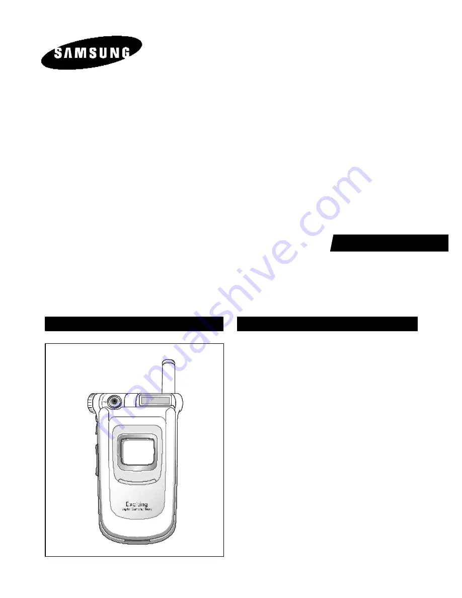
Page 10: ...SUNG Proprietary Contents may change without notice 3 SGH V200 Exploded View and its Parts list 3 1 1 Cellular phone Exploded View 28 1 2 3 4 5 6 7 8 9 16 11 10 17 15 14 13 12 18 19 20 21 22 24 23 25 26 27 ...
Page 11: ...1478 8 SCREW CAP GH73 01052A 9 WINDOW LCD GH72 05929A 10 CAMERA KNOB GH72 03941A 11 CAMERA FPCB GH59 00649A 12 CAMERA SIDE KEY GH71 00719A 13 CAMERA PIECE GH72 03940A 14 CAMERA KNOB SUS GH71 00718A 15 SCREW 6001 001611 16 FRONT COVER GH75 02353A 17 VOLUME KEY GH75 02358A 18 KEYPAD GH75 02356C 19 DOME SHEET GH59 00629A 20 MAIN PBA GH92 01414A 21 MIC GH59 00626A 22 CONNECTOR COVER GH73 01069A 23 ANT...
Page 12: ... change without notice SGH V200 Exploded view and its Part list 3 3 3 Test Jig GH80 00001A 3 1 RF Test Cable GH39 00105A 3 2 Test Cable GH39 00122A 3 3 Serial Cable 3 4 Power Supply Cable 3 5 DATA CABLE GH39 00159A 3 6 TA GH44 00184G ...
Page 13: ...0 2203 005496 C1101 2203 000254 C1102 2203 005061 C1103 2203 005061 C1104 2203 000254 C1105 2404 001100 C1106 2404 001151 C1107 2203 000254 C1108 SEC Code Design LOC 2203 005061 C1109 2203 001598 C111 2203 005482 C1110 2203 005482 C1111 2203 005482 C1112 2203 005061 C1113 2203 005061 C1114 2203 005482 C1115 2203 005481 C1116 2203 005061 C1117 2203 005061 C1118 2203 005061 C1119 2203 001598 C112 22...
Page 14: ...000812 C218 2203 000812 C219 2203 000812 C220 2203 000812 C221 2203 000438 C222 2203 000812 C223 2203 000812 C224 2203 000812 C225 2203 000812 C226 SEC Code Design LOC 2203 000812 C227 2203 000812 C228 2203 000812 C229 2203 000812 C230 2203 000812 C231 2203 005065 C232 2203 005065 C233 2203 000233 C234 2203 000233 C235 2203 000233 C236 2203 005061 C237 2203 000233 C238 2203 000233 C239 2203 000233...
Page 15: ...9 C702 2203 005496 C703 2203 005065 C704 2203 005061 C705 2203 000254 C706 2203 000254 C707 2203 000254 C708 2203 000254 C709 2203 000254 C710 SEC Code Design LOC 2203 000254 C711 2203 000254 C712 2203 000254 C713 2203 000812 C714 2203 000812 C715 2203 000812 C716 2203 000254 C800 2203 000386 C801 2007 007771 C805 2203 001412 C806 2203 000254 C807 2203 000254 C808 2203 000254 C809 2203 005482 C811...
Page 16: ...1 001547 LED817 0601 001547 LED818 0601 001547 LED819 0601 001547 LED820 0601 001547 LED821 4302 001130 M101 2801 004025 OSC601 2809 001260 OSC801 0504 000168 Q100 SEC Code Design LOC 0502 001201 Q101 0501 000225 Q400 2007 001288 R1000 2007 001307 R1001 2007 007008 R1002 2007 007008 R1003 2007 001288 R1004 2007 001307 R1005 2007 007008 R1006 2007 007008 R1007 2007 007107 R1008 2007 001319 R103 200...
Page 17: ...604 2007 007308 R605 2007 000172 R606 2007 000162 R607 2007 000144 R701 2007 007200 R705 2007 007200 R706 2007 000172 R800 2007 001308 R801 SEC Code Design LOC 2007 007405 R802 2007 000138 R805 2007 001306 R806 2007 001306 R807 2007 001306 R808 2007 001306 R809 2007 001306 R810 2007 001306 R811 2007 001306 R812 2007 001306 R813 2007 007008 R814 2007 001306 R815 2007 001306 R816 2007 001306 R818 20...
Page 18: ... 1204 001984 U700 0504 001042 U701 0504 001042 U702 0504 001042 U703 1009 001010 U802 1205 002185 U900 1205 002268 U901 1209 001434 U902 3404 001152 VOL_DN 3404 001152 VOL_UP 0406 001083 ZD300 0406 001083 ZD301 0406 001152 ZD302 1405 001082 ZD303 1405 001082 ZD304 1405 001082 ZD305 1405 001082 ZD306 1405 001082 ZD307 1405 001018 ZD308 1405 001082 ZD401 1405 001082 ZD402 1405 001082 ZD403 1405 0010...
Page 19: ...SAMSUNG Proprietary Contents may change without notice 4 7 SGH V200 Electrical Parts List M ME EM MO O ...
Page 20: ...I4133T π 2 RF PLL PGA SERIAL DATA INTERFACE GSM 890MHz 915MHz PCS 1850MHz 1910MHz PAM GSM 925MHz 960MHz PCS 1930MHz 1990MHz I Q CSP1093 TRIDENT DSP16000 ARM7TDMI UI SERIAL DATA CLK LE RF FILTER DCS 1805MHz 1880MHz L N A PGA A D C A D C IF PLL DCS 1710MHz 1785MHz D E T 100KHz CHANNEL FILTER D A C D A C PGA PGA R X TCVCXO 13 MHz C L K A F C T X I Q SI4201 ...
Page 21: ...128M TXIP TXIN TXQP TXQN RXIP RXIN RXQP RXQN SERCK SERLE SERDA RFOVL TXP OCTL RF DIRVER TXI Q RX I Q TXP SERCK SERLE SERDA OCTL IO RWN AB 8 0 DB 15 0 INT1 IRQx PAx RSTB IO RWN AB 8 0 DB 15 0 INT1 IRQx PAx RSTB ARM JTAG ICE DAICK DAIRN DAIDO DAIDI DAI DSPJTAG JTAG GPRS ACC PPI Programmable Peripheral I O RTC JTAG ICE DSP16000 ARM7TDMI EMI Camera Solution Camera DSP Camera Asic CCD Y 0 7 UV 0 7 PCLK...
Page 22: ... C608 C609 C610 C611 C612 C613 C614 C616 C617 C700 C701 C702 C703 C704 C705 C706 C707 C708 C709 C710 C711 C712 C713 C714 C715 C716 C800 C801 C805 C806 C807 C808 C809 C903 C904 C905 C906 C907 C908 C909 C910 C911 C912 C913 C914 C915 C916 C917 C918 C919 C920 CN100 CN1001 CN1101 CN201 CN300 CN401 D1101 D1102 D1103 F1003 G1 G2 G3 G4 G7 G8 L1000 L1001 L1002 L1003 L1004 L1006 L900 LED200 M101 MAIN_MIC OS...
Page 23: ...615 C811 CLEAR DOWN END_PWR F1 F2 G6 HZREF I LED801 LED802 LED803 LED804 LED805 LED806 LED807 LED808 LED809 LED810 LED811 LED813 LED814 LED815 LED816 LED817 LED818 LED819 LED820 LED821 LEFT MCKI PCLK R200 R307 R503 R603 R604 R605 R806 R807 R808 R809 R810 R811 R812 R813 R814 R815 R816 R818 R819 R820 R821 R822 R823 R824 R825 R826 RIGHT SEND SH T TP200 TP201 TP202 TP203 TP204 TP205 TP206 TP207 TP208 ...
Page 24: ... Charge the Battery pin 15 2 8V Check U100 and C113 pin 46 and pin 39 2 8V Check U100 and C112 Check the clock signal at pin4 of OSC801 Freq 13MHz Vrms 300mV and Check the clock generation circuit related to OSC801 U901 pin 19 END No Yes Yes Yes Yes Yes No No No No pin 13 1 8V No Yes Check the V bat Voltage Check the pin of U100 Check the initial operation Check the current consumption ...
Page 25: ...e problem it has to be replaced END No Yes Is the pin 28 of U100 Low High Yes Check the U601 There is 32 768kHz wave forms at the C614 and C616 Check the LCD Part Yes No No Yes Yes Yes The Voltage is High at the C114 C116 C117 Check the Audio Part No Check the U100 If it has some problem it has to be replaced Check the U700 The pin 22 of U100 is High Check the U100 LCD display is O K No No Yes Yes...
Page 26: ...notice SGH V200 Flow Chart of Troubleshooting 7 3 3 Sim Part Is there any Signals pin 64 65 66 of U100 Insert SIM is displayed on the LCD Check the U601 Check the SIM Card END No Yes Yes Yes No Check the U100 Is there any Signals pin 1 2 3 4 of CN100 ...
Page 27: ...8 of CN300 is TA_VEXT ㆃ 5V Abnormal charging operation The pin 3 of U101 is low Replace TA or Check CN300 Check the U101 Check the Q101 END No Yes Yes Yes No No The pin 3 of Q101 is low The pin 5 of U101 is 3 2 4 2V Check the U101 No Yes No Solder again or change R111 Yes The ICHRG 1V during charging and ㆃ 180mV full charging ...
Page 28: ...SAMSUNG Proprietary Contents may change without notice SGH V200 Flow Chart of Troubleshooting 7 5 CN10 0 ...
Page 29: ...oting 5 Microphone Part Is the assembled status of microphone O K Microphone does not work C409 ㆃ 2 5V Reassemble the microphone Solder the microphone again or Replace C400 R409 C409 R407 R402 R405 END No Yes Yes Yes Yes No Is microphone ok No Check U700 Check the reference voltage on mic path ...
Page 30: ...peaker Are there any signals at the C221 C228 Check LCD or Replace CN201 Check U401 Is there any signals at the pin 5 and pin 7 of U400 END No Yes Yes Yes No No The type of sound from the Speaker is Melody Replace the Speaker Yes No The pin 4 of U400 is No No Yes Yes Yes Check U400 Is there any signals at the pin 3 and pin 9 of U400 The pin 4 of U400 is No Check U700 ...
Page 31: ...SAMSUNG Proprietary Contents may change without notice 7 8 SGH V200 Flow Chart of Troubleshooting ...
Page 32: ...ck the connect CN1101 No Connect the camera module Yes U1104 pin 5 3 0V No Check U1104 and C1134 Yes U1106 pin 4 2 5V Yes No Check U1106 C1135 and R1106 U1102 pin 3 27MHz No Check U1102 and C1126 Yes Check U1109 pin4 has low active signal No Check U1107 U1112 and U1109 Yes Check U1108 pin4 has low active signal Yes No Check U1110 U1111 and U1108 END ...
Page 33: ...ge C1003 C1004 L1001 resolder or change U100pin39 C116 check or resolder U902 CHECK pin 7 13MHz Vp p 860mV OSC801 CHECK pin 4 clean 3V U902 change or resolder U901 CHECK pin 14 23 26 32 clean 2 8V C808 R805 resolder OSC801 change or resolder U100pin46 C114 check or resolder U901 pin3 4 Vp p 240mV U900 CHECK pin6 20 2 8V U900 resolder or change U901 pin1 2 Vp p 250mV U901 resolder or change U900 pi...
Page 34: ...eck U700 check change YES NO U901 pin14 23 26 32 2 8V U100pin46 C114 change or resolder YES U901 pin9 10 12 13 20dBm U901 pin5 6 7 8 1 7V YES U700 change NO NO U1001 change or resolder YES U902pin5 25 28 3V NO U100 pin39 C116 change or resolder NO U902 pin 7 13MHz Vp p 950mV YES U902 pin9 10 11 1213 3V YES YES U901 change or resolder OSC801 pin 3 13MHz Vp p 950mV OSC801 change or resolder U700 che...
Page 35: ...C1005 C1006 L1002 resolder or change U100pin39 C116 check or resolder U902 CHECK pin 7 13MHz Vp p 860mV OSC801 CHECK pin 4 clean 3V U902 change or resolder U901 CHECK pin 14 23 26 32 clean 2 8V R805 C808 change or resolder OSC801 change or resolder U100pin46 C114 check or resolder U901 pin3 4 Vp p 240mV U900 CHECK pin6 20 2 8V U900 resolder or change U901 pin1 2 Vp p 250mV U901 resolder or change ...
Page 36: ...017 F1003 resolder or change C1009 C1010 L1006 resolder or change U100pin39 C116 check or resolder U902 CHECK pin 7 13MHz Vp p 860mV OSC801 CHECK pin 4 clean 3V U902 change or resolder U901 CHECK pin 14 23 26 32 clean 2 8V C808 resolder OSC801 change or resolder U100pin46 C114 check or resolder U901 pin3 4 Vp p 240mV U900 CHECK pin6 20 2 8V U900 resolder or change U901 pin1 2 Vp p 250mV U901 resol...
Page 37: ... check YES U700 check NO U901 pin14 23 26 32 2 8V U100 pin46 C114 change or resolder YES U901 pin9 10 12 13 20dBm U901 pin5 6 7 8 1 7V YES U700 change NO NO U1001 change or resolder YES U902pin5 25 28 3V NO U100 pin39 C116 change or resolder NO U902 pin 7 13MHz Vp p 950mV YES U902 pin9 10 11 1213 3V YES YES U901 change or resolder OSC801 pin 3 13MHz Vp p 950mV OSC801 change or resolder U700 check ...
Page 38: ...SAMSUNG Proprietary Contents may change without notice SGH V200 Flow Chart of Troubleshooting 7 15 ...
Page 39: ...SAMSUNG Proprietary Contents may change without notice 7 16 SGH V200 Flow Chart of Troubleshooting ...
Page 40: ...ELECTRONICS Samsung Electronics Co Ltd February 2003 Printed in Korea Code No GH68 03689A BASIC ⓒ ...