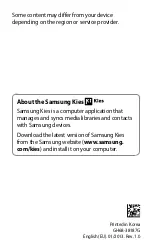
background image

GSM TELEPHONE

SGH-D600E

GSM TELEPHONE

CONTENTS

1.

Specification

2.

Circuit Description

3.

Exploded Views and Parts List

4.

Electrical Parts List

5.

Block Diagrams

6.

PCB Diagrams

7.

Flow Chart of Troubleshooting

Summary of Contents for SGH-D600E

Page 1: ...SM TELEPHONE SGH D600E GSM TELEPHONE CONTENTS 1 Specification 2 Circuit Description 3 Exploded Views and Parts List 4 Electrical Parts List 5 Block Diagrams 6 PCB Diagrams 7 Flow Chart of Troubleshooting ...

Page 2: ... Ltd October 2005 Printed in Korea Code No GH68 08640A BASIC This Service Manual is a property of Samsung Electronics Co Ltd Any unauthorized use of Manual can be punished under applicable International and or domestic law ⓒ ...

Page 3: ...k Downlink 890 915 935 960 880 915 925 960 1710 1785 1805 1880 ARFCN range 1 124 0 124 975 1023 512 885 Tx Rx spacing 45MHz 45MHz 95MHz Mod Bit rate Bit Period 270 833kbps 3 692us 270 833kbps 3 692us 270 833kbps 3 692us Time Slot Period Frame Period 576 9us 4 615ms 576 9us 4 615ms 576 9us 4 615ms Modulation 0 3GMSK 0 3GMSK 0 3GMSK MS Power 33dBm 5dBm 33dBm 5dBm 30dBm 0dBm Power Class 5pcl 19pcl 5p...

Page 4: ...m 11 8 4dBm 12 6 4 dBm 13 4 4 dBm 14 2 5 dBm 15 0 5 dBm TX Power control level DCS1800 0 30 2 dBm 1 28 3 dBm 2 26 3 dBm 3 24 3 dBm 4 22 3 dBm 5 20 3 dBm 6 18 3 dBm 7 16 3 dBm 8 14 3 dBm 9 12 4 dBm 10 10 4 dBm 11 8 4dBm 12 6 4 dBm 13 4 4 dBm 14 2 5 dBm 15 0 5 dBm TX Power control level GSM900 5 33 2 dBm 6 31 3 dBm 7 29 3 dBm 8 27 3 dBm 9 25 3 dBm 10 23 3 dBm 11 21 3 dBm 12 19 3 dBm 13 17 3 dBm 14 1...

Page 5: ... dBm 16 11 5 dBm 17 9 5 dBm 18 7 5 dBm 19 5 5 dBm TX Power control level DCS1800 2 26 4 3 dBm 3 24 3 dBm 4 22 3 dBm 5 20 3 dBm 6 18 3 dBm 7 16 3 dBm 8 12 3 dBm 9 10 3 dBm 10 14 3 dBm 11 12 4 dBm 12 10 4 dBm 13 8 4dBm 14 6 4 dBm 15 4 4 dBm 1 3 GSM EDGE TX power class TX Power control level PCS1900 2 26 4 3 dBm 3 24 3 dBm 4 22 3 dBm 5 20 3 dBm 6 18 3 dBm 7 16 3 dBm 8 12 3 dBm 9 10 3 dBm 10 14 3 dBm ...

Page 6: ...SAMSUNG Proprietary Contents may change without notice This Document can not be used without Samsung s authorization Specification 1 4 ...

Page 7: ...or The oscillator for RX IQ demodulator and Tx modulator are controlled by serial data to select channel and use fast lock mode for GPRS high class operation TRANSCEIVER U102 This chip fully integrated GSM GPRS quad band transceiver with transmit baluns loop filters and most of the passive component in it And also fully integrated fractional N RF synthesizer with AFC control possibility RF VCO wit...

Page 8: ...tor CG generates all clocks for internal and external usage The 32 768 kHz crystal oscillator provides an accurate low clock frequency for the PCF50603 and other circuitry 2 2 2 LCD LCD is consisted of main LCD color 262K TFT LCD Chip select signals in the U301 LCD_MAIN_CS can enable LCD BACKLIGHT signal enables white LED of main LCD 16 bit data lines LD 0 LD 15 transfers data and commands to LCD ...

Page 9: ... are connected to the main speaker via analog switches MIC_P and MIC_N are connected to the main MIC as well EAR1 is the source of External Speaker AK4642 is 16 bit stereo audio CODEC with a built in microphone Amplifier and Headphone Amplifier I2S signals from CL8522S5 are decoded with audio analog signals SAPA1D2 24ELP amplify these signals and deliver to stereo speakers 2 2 8 Memory This system...

Page 10: ...n the ARM core HD 0 15 data lines and HA 0 23 address lines are connected to memory and YMU765 to communicate MV319DNQ Camera DSP Chip controls the communication between ARM core and DSP core OEn WEn control the access of memory KROW and KCOL recognize the key string input status It has J TAG control pins TDI TDO TCK for ARM and DSP core J SEL signal controls different access to ARM and DSP core A...

Page 11: ...3 1 This Document can not be used without Samsung s authorization 3 1 Exploded View QMW01 QFU01 QKP02 QMO01 QLC01 QAU01 QME02 QCR32 QFL01 QSC11 QHI01 QCR26 QPC01 QFR01 QCR32 QKP01 QMP01 QAN02 QME01 QCA02 QCA01 QVK01 QRE01 QCK01 QVO01 QRF01 QCR31 QIF01 QBA01 QAN05 QSP01 QSP02 QAN06 QCR12 ...

Page 12: ...0 EU GH75 07334A QIF01 PMO IF COVER SGH D600 PC UREATHANE B GH72 22629A QKP01 MEC KEYPAD MAIN SGH D600 EU GH75 07207A QKP02 MEC KEYPAD SUB SGH D600 EU C GH75 07206A QLC01 LCD LCD MODULE LTS200QV F03 0 SGH D6 GH07 00734A QME01 UNIT METAL DOME SGH D600 EU 12V GH59 02206A QME02 UNIT KEY PAD SGH D600 HUW9555 010010 GH59 02094A QMO01 MOTOR DC SGHZ130 DMJBRV83CG SGH Z130 GH31 00153B QMP01 PBA MAIN SGHD6...

Page 13: ...M GH74 06456A MPR BOHO VINYL IF SCH X699 3M 4187C GH74 11062A MPR BOHO VINYL S U R SGH D500 STA GH74 13284A MPR SUB BOARD PORON SGH D600 PORON S GH74 14520A MPR MAIN CON INSULATION SGH D600 SP6 GH74 15311A MPR MAIN PBA DOWN L IN SGH D600 SP65 GH74 15312A MPR MAIN PBA DOWN R IN SGH D600 SP65 GH74 15313A MPR MAIN PBA UP L IN SGH D600 SP65 8 GH74 15314A MPR MAIN PBA UP R IN SGH D600 SP65 9 GH74 15315...

Page 14: ...ist 3 4 This Document can not be used without Samsung s authorization 3 3 Test Jig GH80 01909A 3 3 1 RF Test Cable GH39 00283A 3 3 2 Test Cable GH39 00337C 3 3 3 Serial Cable 3 3 4 Power Supply Cable 3 3 5 DATA CABLE GH39 00423A 3 3 6 TA GH44 00954A 3 3 7 TV OUT Cable GH39 00410A ...

Page 15: ...148 C605 C CERAMIC CHIP 2203 000278 C204 C215 C412 C715 C CERAMIC CHIP 2203 000812 C207 C208 C209 C210 C CERAMIC CHIP 2203 005482 C211 C301 C303 C312 C CERAMIC CHIP 2203 006399 C212 C213 C214 C216 C CERAMIC CHIP 2203 005482 C218 C305 C306 C308 C CERAMIC CHIP 2203 005482 C302 C304 C324 C404 C CERAMIC CHIP 2203 006562 C307 C CERAMIC CHIP 2203 000254 C309 C310 C311 C318 C CERAMIC CHIP 2203 005482 C31...

Page 16: ...708 002156 CN701 CONNECTOR HEADER 3711 005643 F100 FILTER 2911 000018 F102 FILTER EMI SMD 2901 001254 F103 FILTER SAW 2904 001553 F300 FILTER DUPLEXER 2909 001279 F500 FILTER EMI SMD 2901 001315 F701 F702 F703 F704 FILTER EMI SMD 2901 001286 F705 FILTER EMI SMD 2901 001286 IFC500 CONNECTOR SOCKET 3710 001994 L101 L103 L109 L122 INDUCTOR SMD 2703 002313 L102 L104 INDUCTOR SMD 2703 002176 L113 INDUC...

Page 17: ...8 R309 R CHIP 2007 000157 R310 R CHIP 2007 007312 R311 R620 R CHIP 2007 007142 R313 R CHIP 2007 007009 R314 R CHIP 2007 001306 R315 R402 R410 R501 R CHIP 2007 000162 R401 R CHIP 2007 008812 R403 R618 R CHIP 2007 007107 R404 R CHIP 2007 007100 R405 R406 R622 U824 R CHIP 2007 000171 R502 R503 R CHIP 2007 000758 R505 R506 R508 R511 R CHIP 2007 000162 R507 R CHIP 2007 000159 R509 R604 R807 R CHIP 2007...

Page 18: ...06 001188 U501 IC 1203 003742 U502 DIODE TVS 0406 001200 U503 IC 1203 003815 U600 IC 1009 001020 U601 IC 1001 001294 U603 U604 IC 1001 001231 U801 IC 1205 002681 U803 IC 1001 001345 U804 IC 1201 002241 U823 IC 1203 003496 U825 COMP SMD NEW IC004 V400 V714 V715 V716 VARISTOR 1405 001082 V500 THERMISTOR 1404 001221 V601 V602 V701 V702 VARISTOR 1405 001138 V703 V704 V705 V706 VARISTOR 1405 001138 V70...

Page 19: ...ung s authorization 5 Block Diagrams 5 1 UAA3587EHN FAR F5EA 897M50 D27CH FAR F5EA 897M50 D27CH FAR F5EA 897M50 D27CH FAR F5EA 897M50 D27CH LMSP54HA 350 BGY290E FESW1 FESW2 FESW3 Tx GSM900 H L L Tx DCS1800 1900 L H L H Rx GSM900 L L L Rx DCS1800 L L L Rx DCS1900 L L H 5 1 RF Solution Block Diagram ...

Page 20: ...SAMSUNG Proprietary Contents may change without notice Block Diagrams This Document can not be used without Samsung s authorization 5 2 5 2 BT Solution Block Diagram ...

Page 21: ...g Circuit Li Ion Battery Slim Standard PCF5213EL1 VIBRATOR SYSTEM CLOCK 26MHz RTC_CLOCK 32 768KHz KEY_BOARD RECEIVER MIC LCD RF INTERFACE D3VDD AVDD VINT PMU D2VDD Serial Data Interface I O Interface A D Interface BB INTERFACE MELODY IC 64 Poly SPEAKER IOVDD VDD_RX_TX VCC_SYN MIC_BIAS CPVDD D1VDD SIMEN GPO VCHG VSAVE SIM CARD MV319DNQ Ext SPEAKER 1G OneNAND MEMORY 5 3 Base Band Solution Block Diag...

Page 22: ...SAMSUNG Proprietary Contents may change without notice Block Diagrams This Document can not be used without Samsung s authorization 5 4 ...

Page 23: ...SAMSUNG Proprietary Contents may change without notice 6 PCB Diagrams 6 1 This Document can not be used without Samsung s authorization 6 1 PCB Top Diagram ...

Page 24: ...SAMSUNG Proprietary Contents may change without notice PCB Diagrams 6 2 This Document can not be used without Samsung s authorization 6 2 PCB Bottom Diagram ...

Page 25: ...s not work Change the Battery END No Yes C408 VINT 2 7V Check the PMU related to VINT No Yes Check the Clock at R404 32KHz Resolder OSC400 No Yes C424 C425 H C424 VDD_IO_HIGH 2 9V C425 VDD_IO_LOW 1 8V Check the related citcuit No Yes C402 VDD_GSM_CORE 1 875V Check the VDD_GSM_CORE circuit No Yes Check for the clock at C116 26MHz No Yes Check the initial operation Yes Yes Check the clock generation...

Page 26: ...23 22 RF1VDD RF2VDD 24 SCL 2 SCN 38 SCP 37 SDA 3 LPVDD 19 MICBIAS 12 NC 53 54 NC OSCI 26 OSCO 25 PWREN1 6 PWREN2 5 GPO1 48 GPO2 47 46 GPO3 18 HCVBAT HCVDD 17 IOD2VBAT 15 14 IOVDD 20 LPD1VBAT CPVDD 35 D1VDD 21 16 D2VDD D3VDD 39 GND 49 50 GND GND 51 52 GND U400 CHGCUR BATMAX 34 CHGDRV 33 CLK32K 4 CPVBAT 36 OSC400 V400 C413 R406 C408 C423 C417 C412 0 R405 C415 POS C426 BAT400 NEG C425 R408 R404 C424 ...

Page 27: ... H6 VCCCLK E9 CLK F8 VCCMASH G8 DCSLNAIB D1 DCSGSM1GND D2 DIVON D8 CLKOUT2 D9 VCCRFVCO B6 DCSLNAI C1 CLK2CONT C8 VCCBB A7 VCCRFSYN A8 VCCBUF A9 VCCMIX B3 CAPIB B4 CAPQB B5 VCCLNA A3 CAPQ A5 VCCRFLO A6 U100 R103 C116 TP100 R102 C120 R105 DCS_RX_N DCS_RX_P RF_CLK D_REF_CLK 26MHz Clock Typical 3 7V 1 8V R401 L401 R403 C403 C401 FB 4 GND 2 1 IN 5 LX 3 _SHDN U402 L402 C402 VDD_IO_HIGH VBAT VDD_GSM_CORE...

Page 28: ...t can not be used without Samsung s authorization Flow Chart of Troubleshooting 7 4 7 2 Initial Is U400 RSTON is HIGH Initial Failure Check the circuit related to reset END No Yes Is U200 R211 R212 OK Yes Yes No Check the U200 Check the 16bit data signal memory CE Yes ...

Page 29: ...WE_E G4 GPIOB2 F2 ADD21 ADD23 F5 OE_R_W E2 KCOL3 E17 KCOL0 D18 KCOL2 D17 KROW2 C17 KCOL1 C18 KROW3 B17 KCOL4 B18 KROW4 A17 KROW1 A18 KROW0 A16 TP212 VDD_IO_LOW TP210 TP211 TP214 TP209 TP208 TP213 6 7 8 R214 12 34 5 HA 24 IMAGE_RST SD_DATA SD_CLK ADVn CS4n_NAND FLASH_LED_EN CS2n_FLASH AUDIO_SEL SD_DETECT EAR_SWITCH SD_CMD JACK_IN USB_CHG_ON HA 23 KEY_ROW 0 4 KEY_ROW 4 KEY_ROW 3 KEY_ROW 2 KEY_ROW 1 ...

Page 30: ...Chart of Troubleshooting 7 6 7 3 Charging Part Check the U501 pin 1 4 9V Abnormal charging part END No Yes U501 pin 5 L No Yes Check the U501 pin 10 4 2V No Yes Check the the circuit related to V_EXT_CHARGE Resolder or replace U501 Check the circuit related to AUX_ON signal Yes U501 pin 8 L Yes No Resolder or replace U501 ...

Page 31: ...e used without Samsung s authorization 7 7 Charging VDD_IO_HIGH BATTERY CHARGING Typical 3 7V 5 0V Typical 1 4V C506 C504 R513 ZD501 R514 C507 R517 C505 3 _PPR R518 11 GND GND 8 9 ICDL 6 IMIN USB 2 USBON 7 _CHG 4 _EN 5 U501 BAT 10 CRDL 1 R512 VBAT AUX_ON END_OF_CHG MES_BATT V_EXT_CHARGE USB_CHG_ON VBUS CHG_ON ...

Page 32: ...tion Flow Chart of Troubleshooting 7 8 7 4 Sim Part CN400 pin 1 5 H Phone can t access SIM Card Check the sim charge pump Check the SIM Card END No Yes Yes Yes No Check the clock After Power ON Check SIMCLK Signal on pin3 of SIM400 in a few second Yes No Replace PBA After SIM card insert CN400 pin 2 H SIM_RST Yes ...

Page 33: ...ts may change without notice Flow Chart of Troubleshooting This Document can not be used without Samsung s authorization 7 9 SIM P M U SIM_VCC SIM_CLK SIM_RST SIM_IO C419 C422 C418 7 8 G G 9 10 G SIM400 1 2 3 4 5 6 G 2 292292 7 ...

Page 34: ...s authorization Flow Chart of Troubleshooting 7 10 7 5 Microphone Part Check the connection from MIC Check the circuit from U200 to MIC Resolder MIC Resolder the C602 C604 L600 and L601 END No Yes Yes Yes Yes No U601 is OK No Check the U601 Microphone does not work Yes Check the MIC No Replace the MIC ...

Page 35: ...authorization 7 11 Microphone C602 C601 1 2 3 4 5 6 78 ZD600 R604 C605 C606 R605 MIC_BIAS C603 L602 NO1 10 NO2 1 VCC C608 COM2 9 11 GND 6 GND 4 IN1 8 IN2 NC1 5 NC2 7 2 U601 COM1 3 MIC_BIAS C607 L601 R601 C604 MIC600 MIC_N MIC_P MIC_SEL MIC_SEL_N MIC_IN_N AUXM_N MIC_SEL_P MIC_IN_P AUXM_P MIC_SEL_N MIC_IN_P MIC_IN_P MIC_SEL_P MIC_IN_N ...

Page 36: ...7 pins of U801 are OK Stereo Speaker does not work Check the signal at 25 26 pins of U801 Check the supply voltage of U301 U801 3 3V Check 27MHz clock of OSC300 END No Yes No Check the signal at 4 16 pins of U803 Check 10 pin of U803 is 1 8V Yes No Check the PWM signal at 4 6 16 18 of U804 Change U804 D class Audio AMP Yes No Check the Speaker contact pins No Yes Peplace Speaker inside Intena Yes ...

Page 37: ...R Typical 3 7V C812 L806 L804 R811 R812 VDD C814 NC NC 27 3 VDD 4 VOMR 5 VSS 6 VOPR 7 VDD 8 VSS 9 VDD 2 VSS 20 VSS 21 VDD 22 VIML 23 VREFL 24 VIPL GND 25 26 VREFR 12 VIPR 13 EN_R 14 VSS 15 VDD 16 VOML 17 VSS 18 VOPL 19 TP506 U804 1 EN_L 10 VIMR 11 TP505 TP503 TP504 R805 R806 L810 L813 L812 C811 C828 C821 VBAT C813 L801 C804 C805 C827 R810 R813 C816 C815 L803 L809 R804 C822 L807 AMP_EN SPK_R J_SPK ...

Page 38: ...t Samsung s authorization Flow Chart of Troubleshooting 7 14 7 7 Key Data Input When one of the keys is pushed KEY_ROW 0 4 KEY_COL 0 4 signal is OK Yes No Replace the PBA Check Initial Operation Yes Yes No END Check the Dome sheet Key Pad When one of the keys is pushed is it displayed on LCD ...

Page 39: ...out Samsung s authorization 7 15 7 8 Receiver Part Check signal at V717 V718 Chane PBA END No Yes Yes Receiver does not work Yes No Change LCD Module Yes No Resoldering of the wire Check the soldering at SPK SPK PAD of the LCD Module Yes Is it working No change Receiver Check the signal at SPK SPK PAD of the LCD Module ...

Page 40: ...SAMSUNG Proprietary Contents may change without notice This Document can not be used without Samsung s authorization Flow Chart of Troubleshooting 7 16 ...

Page 41: ... This Document can not be used without Samsung s authorization 7 17 7 9 LCD Part 5 pin of LCD backlight IC U102 is high Replace the LCD backlight IC END No Yes Yes LCD does not work Check the board to board FPC Change the board to board FPC No Yes Is it working Check LCD Module No Yes ...

Page 42: ...s authorization Flow Chart of Troubleshooting 7 18 C24 C37 1 R14 ZD5 1 2 C19 C23 R6 VBAT 21 22 NC OUT 2 SET 3 20 IN 14 11 LED1 LED2 10 LED3 9 LED4 8 LED5 7 LED6 6 NC 1 CIN 13 ENM 5 ENS 4 GND 12 17 GND GND 18 19 GND GND U102 C1P 16 C2N 15 C2P C21 C22 C20 C25 BACKLIGHT LED_C4 LED_C3 LED_C2 LED_C1 LED_OUT ...

Page 43: ...Samsung s authorization 7 19 7 10 Camera part Camera function does not work Yes No Reconnect the camera module Check the Camera connector on LCD module Yes Check the voltage of L701 2 8V No Check U305 Yes Check the 5 7 pins clock of CN701 No Check the related circuit of U301 Yes Is it working No Change Camera Module END Yes ...

Page 44: ...f Troubleshooting 7 20 7 11 Trans Flash Card part T Flash card does not work Yes No Check 6 pin of U503 it should be high Check the 5 pin of U503 3 3V Yes Check the clock at 4 pin of U504 No Check the related circuit Yes Check the 2 pin of CN500 is high No Check the related circuit Yes Is it working No Change T Flash Card END Yes ...

Page 45: ...ment can not be used without Samsung s authorization 7 21 7 12 TV OUT TV out does not work Yes No Replace the U306 Check the 4 pin of U306 Yes Check the TV out setting is correctly NTSC or No Check the Menu Setting DISPLAY TV out Yes Other multimedia function work well No Change the PBA Yes END ...

Page 46: ...D0 H11 M_SD1 F13 M_SD6 F14 M_SD4 F2 C_PWDN F4 C_D7 F5 VDDI G1 GPIO2_D15 G10 M_SD5 G11 M_SD7 E5 C_D4 E6 SD_D5_SD_3 E7 M_INTR E8 M_SD13 E9 M_SA1 F1 VSS F10 M_SD8 F11 M_SD9 D9 XRTS0 E1 C_D6 E10 M_SD12 E11 M_SD14 E13 M_SD10 E14 M_SD11 E2 C_D5 E4 C_D1 D13 M_SD15 D14 M_SA0 D2 C_D2 D4 C_PCLK D5 VDDS D6 SD_D2_SD_0 D7 M_ADS D8 VDDC B9 VSS C1 C_D0 C13 XOUT C14 XIN C2 C_MCLK D1 C_D3 D10 M_HOLD D11 MS_CS_N B1...

Page 47: ...is Document can not be used without Samsung s authorization 7 23 7 13 Bluetooth part END Yes Change the Bluetooth Module No Is it working Yes Check the contact pin No Check the contact of Bluetooth Intenna Yes Check the 15 pin of U302 is high Change the U302 No Yes Bluetooth does not work ...

Page 48: ...UART_RXD 6 REQ_CTRL 7 EEPROM_CLK COEX_3 8 VDD_IO 9 ANT 29 GND 3 USB_DN 30 UART_CTS_N 31 PCM_OUT 32 UART_RTS_N 33 PCM_IN 34 UART_TXD 35 TM3_LOW 21 VDD_RF 22 RESET_N 23 TX_PU_TDD_N 24 GND 25 PCM_SYNC 26 GND 27 GND 28 EEPROM_DATA GPIO_6 14 HOST_WAKE 15 BT_WAKE 16 TM0_HIGH 17 GND 18 GND 19 TM1 2_HIGH 2 VDD_USB 20 U302 1 PCM_BCLK 10 XTAL_PD COEX_1 11 USB_DETACH GPIO_7 12 LPO_IN 13 VDD_IO_LOW TP317 R308...

Page 49: ...ow Chart of Troubleshooting This Document can not be used without Samsung s authorization 7 25 7 14 Main Key LED part END Yes Is it working Yes Check the R612 R613 R614 R615 Yes Check the 6 pin of U602 is high Check the U602 No Yes Main key LED does not work ...

Page 50: ...es Yes Yes Yes C144 C145 1V Resolder U102 Check Resolder U102 R103 R105 R106 RF26MHz RF PSU Part Check U102 pin23 26 28 31 2 7V U102 pin7 8 9 10 1V END No No No Yes Yes Yes Resolder C119 C121 L114 Resolder F100 Check ANT Switch control circuit U102 pin29 70dBm pin30 70dBm F100 pin5 pin6 65dBm Check F100 pin9 10 12 L RX ON RF input 62CH Amp 50dBm Yes No Resolder CN100 C146 F100 pin8 65dBm ...

Page 51: ...F100 pin11 18dBm Check F100 pin10 H 2 68V pin9 pin12 L No Yes Check ANT Switch control circuit Yes Change or Resolder F100 No U103 pin16 18dBm Yes Resolder L116 C131 Check U102 VBAT pin7 14 OK No U103 pin12 11dBm Yes Yes Resolder or Change U103 Check VBAT or U103 control signal No No U102 pin7 8 9 10 1V Check U102 pin23 26 28 31 2 7V OK No No Check Resolder U102 R103 R105 R106 RF26MHz RF PSU Part ...

Page 52: ...s Yes Yes Yes C144 C145 1V Resolder U102 Check Resolder U102 R103 R105 R106 RF26MHz RF PSU Part Check U102 pin23 26 28 31 2 7V U102 pin7 8 9 10 1V END No No No Yes Yes Yes Resolder C111 C115 L113 Resolder F100 Check ANT Switch control circuit U102 pin35 70dBm pin36 70dBm F100 pin1 pin2 65dBm Check F100 pin9 10 12 L RX ON RF input 698CH Amp 50dBm Yes No Resolder CN100 C146 F100 pin8 65dBm ...

Page 53: ...Yes Yes Yes C144 C145 1V Resolder U102 Check Resolder U102 R103 R105 R106 RF26MHz RF PSU Part Check U100 pin23 26 28 31 2 7V U102 pin7 8 9 10 1V END No No No Yes Yes Yes Resolder L102 L104 C100 Resolder F100 Check ANT Switch control circuit U102 pin32 70dBm pin33 70dBm F100 pin3 pin4 65dBm Check F100 pin9 H pin10 12 L RX ON RF input 661CH Amp 50dBm Yes No Resolder CN100 C146 F100 pin8 65dBm ...

Page 54: ...100 pin13 18dBm Check F100 pin12 H 2 68V pin9 pin10 L No Yes Check ANT Switch control circuit Yes Change or Resolder F100 No U103 pin18 18dBm Yes Resolder L126 C133 U824 Check U103 VBAT pin7 14 OK No U103 pin4 11dBm Yes Yes Resolder or Change U103 Check VBAT or U103 control signal No No U102 pin7 8 9 10 1V Check U102 pin23 26 28 31 2 7V OK No No Check Resolder U102 R103 R105 R106 RF26MHz RF PSU Pa...

Page 55: ...B RFOUT_LB 16 VBAND 9 2 VBAT1 VBAT2 3 13 VBAT3 VBAT4 U103 17 G G 15 1 G G 19 5 MODE 4 L117 L118 R114 R111 VCC_SYN L124 R116 C140 C149 C110 28 VCCSYN 23 VDDL 16 L126 REFIN 21 REFVCC 19 25 RFTUNE 32 SWBIA 33 SWBIB 40 SWON 39 TXVCC VCCCP 26 11 VCCIF VCCRF 31 VCCRFLO 2 8 IA 7 IB LBIA 29 30 LBIB 38 LBO 45 NC1 NC2 46 PGMDIV 17 QA 10 QB 9 4243 GND3 GND4 44 15 GNDL 22 GNDREF 34 GNDRF1 1 GNDRF3 GNDRF4 3 37...

Page 56: ...SAMSUNG Proprietary Contents may change without notice This Document can not be used without Samsung s authorization Flow Chart of Troubleshooting 7 32 ...

Reviews: