5 Troubleshooting
5-8
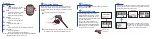
PG17N*/PG19N*
IC101 (17”: IC104, Pin12) Pin 15
input exists and
varies with different patterns?
Check and replace IC101 (17”:IC104).
Input full white pattern to monitor.
No
Yes
T501 Pin 8 output exists?
Check and replace T501.
Yes
No
IC103 (17”: IC04) Pin 16 output
exists and varies with different
patterns?
Check and replace IC103 (17”: IC04).
Yes
No
Check and replace Q101,
Q102 and +12 V line.
Check CN102.
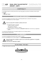
5-1-14 ABL Failure
5-1-15 Dynamic Focus Failure
IC261 Pin 32 and IC250 Pin 7
output are right?
Check and replace IC250 and IC261.
Yes
No
Some parts around Q551,
Q552, Q553 and Q554 are right?
Replace failed part.
Yes
No
Some parts around T502 are right?
Replace failed part.
Check the connection between FBT
Pin 13, CRT Socket PCB.
Yes
No
8
WAVEFORMS
28
28
4.48 V (IC103, #16)
CH1 P-P = 4.48 V
CH1 RMS = 2.652 V
8
960 mV (IC261, #32)
CH1 P-P = 960 mV
CH1 RMS = 6.042 V
Summary of Contents for PG19N
Page 2: ...Samsung Electronics Co Ltd April 2000 Printed in Korea P N BH68 00129F 01...
Page 17: ...Memo 4 Alignment and Adjustments 4 8 PG17N PG19N...
Page 67: ...Memo 8 Block Diagrams 8 2 PG17N PG19N...
Page 71: ...10 Schematic Diagrams 10 3 PG17N PG19N 10 2 Micom Part Schematic Diagram 4 6 3 5...
Page 73: ...10 Schematic Diagrams 10 5 PG17N PG19N 10 3 H V Process Part Schematic Diagram 9 11 10 7 8...
Page 77: ...10 Schematic Diagrams 10 9 PG17N PG19N 18 21 20 19 10 5 HIGH VOLTAGE Parts Schematic Diagram...
Page 79: ...10 Schematic Diagrams 10 11 PG17N PG19N 10 6 Video Parts Schematic Diagram 17...