


7-2
Samsung Electronics
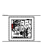
Schematic Diagram
This Document can not be used without Samsung’s authorization.
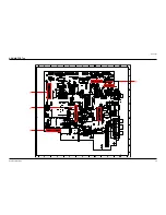
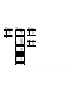
7-1 Overall Block Diagram
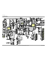
A24/A25 Block Diagram
ANT
AUX-L
AUX-L
TUNER-L
TUNER-R
TAPE-L
TAPE-R
CD-L
CD-R
AC CORD
HEAD
PHONE
SPK-L
SPK-R
MCW12
L-CH
R-CH
CE CLK DATA
CE CLK DATA
VFD CONTROL
VP
VFD+
VFD-
CD-ON
P-SENSE
5.6V
P-ON
GND
12V
VCC-
VCC-
GND
GND
VCC+
VCC+
TUNER
PACK
TAPE
DECK
CD/MP3/WMA
DECK
SMPS
VFD
MICOM IC
HIC2
4556
UIC2
FRONT PCB
PT6315
FIC1
FUNCTION IC
R2S15904
AAIC1
AMPLIFER IC
TDA8922BJ
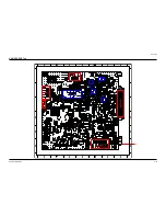
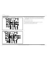
DA25 Block Diagram
ANT
AUX-L
AUX-L
TUNER-L
TUNER-R
TAPE-L
TAPE-R
CD-L
CD-R
AC CORD
HEAD
PHONE
PCW13
(MAIN)
R-CH
L-CH
CE CLK DATA
CE CLK DATA
VFD CONTROL
VP
VFD+
VFD-
CD-ON
P-SENSE
5.6V
P-ON
GND
12V
VCC-
VCC-
GND
GND
VCC+
VCC+
TUNER
PACK
TAPE
DECK
CD/MP3/WMA
DECK
SMPS
VFD
MIC
MICOM IC
HIC2
4556
UIC2
FRONT PCB
PT6315
FIC1
FUNCTION IC
R2S15904
FIC2
4558
SPK-L
SPK-R
AAIC1
AMPLIFER IC
TDA8922BJ
AGND
MIC SIGNAL
A10V EGND EGND 3.3V
5.0V MGND M8V
Main System MICOM control Function IC (R2S15904), Tuner pack, Tape deck IC (HA12237F), CD/DVD DECK.
It gets all information from R2S15904. They have a communication among them with the HOST ↔ SLAVE interface.
And Main System MICOM gets the information from User’s remote control. So whenever it gets the information, it
displays it on the VFD.
PCW3 on MAIN PCB gets power from SMPS;
PCN1A on DVD PCB gets power from SMPS;
The CD Deck, Tape Deck, AUX Jack and Tuner Pack GND are each connected to Function IC (R2s15904).
Then GND after processing. The Data will be sent to AMP IC VCC+ (AAIC1).
Headphone IC (4556) gets signal from Function and output it to H/P JACK.
Summary of Contents for MM-DA25
Page 34: ...Samsung Electronics 6 3 PCB Diagram 6 2 MIC PCB Top 1 2 MCON11 UJ2 ...
Page 36: ...Samsung Electronics 6 5 PCB Diagram 6 3 MIC PCB Bottom MCON11 UJ2 ...
Page 37: ...6 6 Samsung Electronics PCB Diagram 1 2 6 4 FRONT PCB Top MCW1 VFD1 UJ11 ...
Page 39: ...6 8 Samsung Electronics PCB Diagram 6 5 FRONT PCB Bottom MCW1 VFD1 UJ11 UIC2 HIC2 MIC1 ...
Page 43: ...6 12 Samsung Electronics PCB Diagram 6 7 1 Test Point Wave Form TP1 TP2 ...
Page 46: ...Samsung Electronics 6 15 PCB Diagram 6 9 MPEG PCB Bottom MIC1 BIC4 DIC3 VIC1 IC4 IC3 IC2 ...
Page 47: ...6 16 Samsung Electronics PCB Diagram 1 6 10 SMPS PCB Top CON3 IC1 ...
Page 49: ...6 18 Samsung Electronics PCB Diagram 6 11 SMPS PCB Bottom CON3 ...


