background image

10 Operating Instructions and Installation

10-3

3.

HDMI IN 1,HDMI IN 2, HDMI IN 3

- Supports connections between HDMI-connection-enabled AV devices (Set-Top Boxes, DVD players)
- No additional Audio connection is needed for an HDMI to HDMI connection.

What is HDMI? 
-"High Definition Multimedia interface" allows the transmission of high definition digital video data and 

multiple channels of digital audio (5.1 channels). 

-The HDMI/DVI terminal supports DVI connection to an extended device with the appropriate cable (not supplied). 

The difference between HDMI and DVI is that the HDMI device is smaller in size, has the HDCP 
(High Bandwidth Digital Copy Protection) coding feature installed, and supports multi - channel digital audio. 

The external devices that support lower versioned HDMI mode may not implement sound output
for the TV with the latest HDMI version (HDMI 1.3).
In this case, connect to HDMI IN 2 and DVI IN (HDMI 2) "R - AUDIO - L" on the back panel of the TV.
Part of lower versioned HDMI cables may cause annoying flickers or no screen display.
In this case use the cable that supports the latest HDMI version (HDMI 1.3).

DVI IN (HDMI 2) (AUDIO R/L)

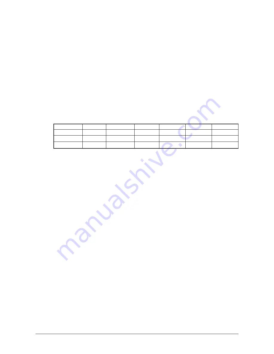
-  When connecting this product via HDMI or DVI to a Set Top Box, DVD Player or Games Console

etc, make sure that it has been set to a compatible video output mode as shown in the table
below. Failure to observe this may result in picture distortion, image breakup or no picture.

- When using an HDMI/DVI cable connection, it is only possible from the HDMI 2 terminal.

The exteYou should use the DVI-to-HDMI cable or DVI-HDMI Adapter for the connection, and the 
"R - AUDIO - L" terminal on DVI for sound output.

Supported modes for HDMI/DVI and Component

4.

Connecting an Aerial or Cable Television Network 

To view television channels correctly, a signal must be received by the set from one of the following sources:
-  An outdoor aerial / A cable television network / A satellite network

5.

Connecting CI (Common Interface) CARD

-  When not inserting "CI CARD" in some channels,"Scrambled Signal" is displayed on the screen.
-  The pairing information containing a telephone number, CI CARD ID, Host ID and other information will be 

displayed in about 2~3 minutes. If an error message is displayed, please contact your service provider.

-  When the channel information configuration has finished, the message "Updating Completed" is displayed, 

indicating that the channel list is now updated.

.  You must obtain a CI CARD from a local cable service provider. 

Remove the CI CARD by carefully pulling it out with your hands since dropping the CI CARD
may cause damage to it.

.  Insert the CI-Card in the direction marked on it.

7.

Connecting External A/V Devices 

-  Connect RCA or S-VIDEO cable to an appropriate external A/V device such as VCR, DVD or Camcorder. 
-  Connect RCA audio cables to "R - AUDIO - L" on the rear of your set and the other ends to corresponding audio 

out connectors on the A/V device. 

-  Headphone may be connected to the headphone output ( 

) on the rear of your set. While the headphone is 

connected, the sound from the built-in speakers will be disabled. 

8.

Connecting Computer 

-  Connect the D- Sub cable (optional) to "PC (PC IN)" on the rear of your set and the other end to the Video Card 

of your computer. 

-  Connect the stereo audio cable (optional) to "AUDIO (PC IN)" on the rear of your set and the other end to "Audio 

Out" of the sound card on your computer. 

9.

DIGITAL AUDIO OUT (OPTICAL) 

-  Connect to a Digital Audio Component. 

10. SERVICE 

-  Service connection for qualified service engineer.

480i

480p

576i

576p

720p

1080i

HDMI/DVI 50Hz

X

X

X

O

O

O

HDMI/DVI 60Hz

X

O

X

X

O

O

Component

O

O

O

O

O

O

Summary of Contents for LE37M87BDX

Page 1: ...40SEN GTU46SEN GTU52SEN Model LE37M87BDX LE40M87BDX LE46M87BDX LE52M87BDX Manual SERVICE TFT LCD TV Fashion Feature Luxurious Slim Design Supreme Picture Quality Supreme Sound Quality Supreme Convenience Quality Convenience for Users ...

Page 2: ...amsung Electronics Co Ltd LE37M87BDX LE40M87BDX LE46M87BDX LE52M87BDX Service Manual First edition June 2007 Printed in Korea Trademarks Samsung is the registered trademark of Samsung Electronics Co Ltd LE37M87BDX LE40M87BDX LE46M87BDX LE52M87BDX and MacMaster Cable Adapter are trademarks of Samsung Electronics Co Ltd Macintosh Power Macintosh are trademarks of Apple Computer Inc All other tradema...

Page 3: ...ts and Adjustments 3 3 1 3 1 Service Instruction 3 1 3 2 How to Access Service Mode 3 2 3 3 Factory Data 3 3 3 4 Service Adjustment 3 7 3 5 White Ratio Balance Adjustment 3 9 3 6 Servicing Information 3 10 4 4 Trouble shooting 4 4 1 4 1 First Checklist for Troubleshooting 4 1 4 2 Checkpoints by Error Mode 4 2 5 5 Exploded View and Parts List 5 5 1 5 1 LE37M87BDX Exploded View 5 1 5 2 LE37M87BDX Pa...

Page 4: ...nd Installation 1 10 1 10 1 Front 10 1 10 2 Connection Panel 10 2 10 3 Remote Control 10 4 10 4 Installing the Stand 10 5 10 5 Installing the Wall Mount Kit 10 5 1 11 Disassembly and Reassembly 1 11 1 11 1 Disassembly 11 1 11 2 Reassembly 11 5 1 12 PCB Diagram 1 12 1 12 1 Main PCB Layout 12 1 12 2 IP Board Diagram 12 2 1 13 Circuit Descriptions 1 13 1 13 1 Block description 13 1 13 2 Main Block 13...

Page 5: ... City Gyeonggi Do Korea 443 742 Printed in Korea P N BN82 00191A 00 URL http itself sec samsung co kr This Service Manual is a property of Samsung Electronics Co Ltd Any unauthorized use of Manual can be punished under applicable International and or domestic law ...

Page 6: ...hing is essential 4 Avoid overload Excessive signal from a sweep generator might overload the front end of the TV When inserting signal markers do not allow the marker generator to distort test result 5 Connect the TV only to an AC power source with voltage and frequency as specified on the backcover nameplate 6 Do not attempt to connect or disconnect any wire while the TV is turned on Make sure t...

Page 7: ... Right Menu Enter Number Key 0 9 2 Function Control Key Power CH CH VOL VOL Menu TV VIDEO Enter 3 2 2 Panel Check You have to check Panel Maker Because of different adjustments as follows First of all Check the label rating 1 Label Rating File LCD PANEL MARK A ACER AUO S SEC C CMO If not printed you could consider S sec panel mark 2 If Panel Mark is A Set the factory mode indicating as follows Opt...

Page 8: ... 3 PC Calibration 4 HDMI Calibration 2 Option Table XXXX XXXX No Item 1 2 3 4 5 6 7 8 9 10 11 12 13 14 15 16 17 18 19 Ready Inch Option Panel Vender Gamma Panel Type Model Option Tuner Tuner TOP Auto Power Nordic LNA Menu TTX On Off TTX List Carrier Mute High Deviation VOL Curve HDMI Hotplug HDMI Clock CtrI HDMI Hotplug Dly ON OFF 23 26 32 AUO CMO ON OFF Normal1 Normal2 Calla Lily Bord Plus Jasmin...

Page 9: ...128 128 128 128 128 128 128 128 128 128 128 128 128 128 128 128 128 128 128 128 128 128 128 128 128 TV AV Scart Comp iDTV PC HDMI 4 SVP PX 1 ComB Filter 2 Sharpness No 1 Item Y Filter Range 00H FFH No 1 2 3 4 5 6 7 8 9 10 11 Item H2Gain H4Gain V2Gain V4Gain Sr2Gain Sr4Gain Sl2Gain Sl4Gain Peakth1 Peakth2 Peskth3 Range 00 1FH 00 1FH 00 1FH 00 1FH 00 1FH 00 1FH 00 1FH 00 1FH 00H FFH 00H FFH 00H FFH ...

Page 10: ... 2 3 4 AV ADC COMP ADC PC ADC ALL RGB 00H FFH 00H FFH 00H FFH 00H FFH 10H 10H 10H 01H DCH EBH DCH EBH 02H 02H 04H 0AH low high Delta No Item Range 1 2 3 4 5 6 7 8 9 10 11 12 13 TCD3 Contrast TCD3 Brightness TCD3 CR TCD3 CB TCD3 Delay Analog Y Offset Analog PB Offset Analog PR Offset Analog Y Gain Analog PB Gain Analog PR Gain Black Level Svp Brightness 00H FFH 00H FFH 00H FFH 00H FFH 00H FFH 00H F...

Page 11: ... FFH 00H FFH 00H FFH Reddish 00H 00H 00H No Item Range 1 2 3 4 5 6 7 8 9 10 11 12 13 14 15 16 OUTCON GAMMA OCC_MODE FALLBACK DBG_MARK SPR_CBR BIT_EXPAND INV_BIT_EXPAND REPEAT_MODE DEMO_ON_OFF MMU_RD_START ME_RD_START MC_RD_START CMZL 0x36E BLOL 0x2A7 LOGO 0x2A7 1 3 1 7 0 1 0 1 0 1 0 1 0 1 0 1 0 1 0 1 00H FFH 00H FFH 00H FFH 00H 0FH 00H 0FH 00H 0FH 0 0 0 0 0 0 0 0 0 0 00H 00H 00H 0H 0H 0H ...

Page 12: ...128 15 30 130 1 165 140 128 128 115 128 128 128 128 0 1 44 20 120 128 20 40 100 200 56 128 128 15 30 130 1 165 140 128 128 128 128 128 128 128 0 1 44 20 120 128 20 40 100 200 56 128 128 15 30 130 1 165 140 128 128 128 128 128 128 128 3 FBE2 No Item Range 0 1 64 20 120 128 55 65 75 225 85 128 128 15 30 130 1 165 128 128 128 150 128 128 128 128 HDMI 0 1 64 20 120 128 75 88 75 225 85 128 128 15 30 13...

Page 13: ...V5810 NTP3000 No Item Range 1 2 3 4 5 6 7 ID Tone Shift ID Tone Thresh Demod Prescaler Master Volume PWM Modulation DRC Threshold Speaker EQ 1H FH 00H FFH 00H 20H 00H 30H 80H F2H 00H 7FH ON OFF 01H 7FH 13H 13H F1H 06H OFF 7 YC Delay No Item Range 1 2 3 4 5 6 7 8 9 10 11 12 13 RF PAL B G RF PAL D K RF PAL I RF SECAM B G RF SECAM D K RF SECAM L L RF NTSC 3 58 RF NTSC 4 43 AV PAL AV SECAM AV NTSC 3 5...

Page 14: ... W2_B_OFFS NO_RGAIN NO_BGAIN NO_R_OFFS NO_B_OFFS C2_RGAIN C2_BGAIN C2_R_OFFS C2_B_OFFS Movie Contr Movie Brigh Movie Color Movie Sharp ON OFF Movie 0 255 0 255 0 255 0 255 0 255 0 255 0 255 0 255 0 255 0 255 0 255 0 255 0 255 0 255 0 255 0 255 0 255 0 255 0 100 0 100 0 100 0 100 No Item Range OFF Movie Cool1 128 128 157 76 119 138 142 48 129 143 141 104 126 136 124 142 128 128 100 45 55 75 TV AV S...

Page 15: ...djustments 3 10 11 Checksum 7A72 12 Reset 13 Spread Spectrun No Item Range 1 2 3 4 5 6 7 8 Spectrum Delta Positive Negative Speed Time FBE Spectrum FEE Delta ON OFF 128 128 0 99 0 99 0 7 0 7 ON OFF 0 5 ON 0 8 2 0 4 OFF 0 ...

Page 16: ...e Adjustment If picture color is wrong check White Balance condition Equipment CA210 Patten Flat W B Pattern Adjust W B in Factory Mode Sub brightness and R G B Offset controls low light region Sub contrast and R G B Gain controls high light region Source AV PAL composite Component 1280 720 60Hz HDMI DVI 1280 720 60Hz Flat W B Pattern Test Pattern MIK K 7256 PAttern 92 Color temperature 1500K 500 ...

Page 17: ... input to the mode in which the adjustment will be made RF DTV PC DVI Input signal VIDEO Mode Model 2 744 484 Mode Pattern 16 DTV DVI Mode Model 6 1280 720 Mode Pattern 16 HDMI Mode Model 6 1280 720 Mode Pattern 16 b Enter factory color control confirm the data c Adjust the low light Refer to table 1 2 in adjustment position by mode Adjust sub Brightness to set the Y value Adjust red offset x and ...

Page 18: ...just the high light Refer to table 1 2 in adjustment position by mode Adjust red gain x and blue gain y to the color coordinates Do not adjust the green gain and sub contrast Y data Picture 4 3 Flat W B Pattern High light Measurement point ...

Page 19: ...pgrade 3 5 1 How to Update Flash ROM 1 Install the Flash Downloader ConnectSet Service Jack and Jig Cable to execute Program Update 2 Flash Downloader program update Before Turning on the set Click connect which is under of OSD Screen Turn on the Set ...

Page 20: ...7 Block Diagrams 7 1 7 Block Diagram This Document can not be used without Samsung s authorization ...

Page 21: ...7 Block Diagrams 7 2 Memo ...

Page 22: ...cuit Descriptions 13 1 13 Circuit Descriptions 13 1 Block description Mosel consists of three main blocks 1 Main board Video signal processing 2 IP board Power supply Inverter 3 T con board LCD Panel control ...

Page 23: ...13 Circuit Descriptions 13 2 Mosel consists of three main blocks 1 Main board Video signal processing 2 SMPS Power supply 3 T con board LCD Panel control ...

Page 24: ...13 Circuit Descriptions 13 3 13 2 Main Block ...

Page 25: ...13 Circuit Descriptions 13 4 13 3 IP Board ...

Page 26: ...ntains electrostatically sensitive devices Use caution when handling these components 11 1 Disassembly LE40F71BX Cautions 1 Disconnect the monitor from the power source before disassembly 2 Follow these directions carefully never use metal instruments to pry apart the cabinet Description Picture Description 1 Place monitor face down on cushioned table Remove screws from the Stand Remove stand ...

Page 27: ...11 Disassembly and Reassembly 11 2 3 Disconnet cables from the main and power boards Description Picture Description 2 Remove screws from the rear cover and lift up the rear cover ...

Page 28: ...11 Disassembly and Reassembly 11 3 5 Lift up the speakers Remove screws from the BRKT Description Picture Description 4 Remove screws from the boards and stand BRKT ...

Page 29: ...11 Disassembly and Reassembly 11 4 7 Remove Panel Front Description Picture Description 6 Lift up the Panel ...

Page 30: ...11 Disassembly and Reassembly 11 5 11 2 Reassembly Reassembly procedures are in the reverse order of disassembly procedures ...

Page 31: ...11 Disassembly and Reassembly 11 6 Memo ...

Page 32: ... 6002 001294 SCREW TAPPING BH M4 L16 ZPC BLK 13 S A 2 T0081 6002 001294 SCREW TAPPING BH M4 L16 ZPC BLK 1 S A 2 M0013 BN96 04746A ASSY COVER P REAR 40M81 EO IDTV ABS PMM 1 S A 3 M0081 6003 001188 SCREW TAPTITE BH B M4 L10 ZPC WHT S 2 S N A 3 CCM1 BN63 02183G COVER SHEET Rhcm PE Vinyl T0 05 1100mm 2 0 99 S N A 3 M0006 BN63 03038A COVER REAR 40M81 EO IDTV ABS PMMA 1 S N A 3 T0071 BN64 00555B INLAY T...

Page 33: ...0 380MIL 20X20X9 5T 1 S N A 3 T0174 BN97 01794A ASSY SMD LE40M87BDX 72 1 S N A 4 SUB05 0202 001477 SOLDER CREAM LST309 M D20 45 96 5Sn 4 894 S N A 4 D1107 0401 000133 DIODE SWITCHING RLS4148 75V 150mA LL 34 1 S A 4 D1204 0401 000133 DIODE SWITCHING RLS4148 75V 150mA LL 34 1 S A 4 D1208 0401 000133 DIODE SWITCHING RLS4148 75V 150mA LL 34 1 S A 4 D1210 0401 000133 DIODE SWITCHING RLS4148 75V 150mA L...

Page 34: ...HING MMBD4148SE 100V 200mA SO 1 S A 4 D1650 0401 001056 DIODE SWITCHING MMBD4148SE 100V 200mA SO 1 S A 4 D1653 0401 001056 DIODE SWITCHING MMBD4148SE 100V 200mA SO 1 S A 4 D1808 0401 001056 DIODE SWITCHING MMBD4148SE 100V 200mA SO 1 S A 4 D1507 0401 001099 DIODE SWITCHING 1N4148WS 75V 150mA SOD 3 1 S A 4 D1508 0401 001099 DIODE SWITCHING 1N4148WS 75V 150mA SOD 3 1 S A 4 D1509 0401 001099 DIODE SWI...

Page 35: ...1 S A 4 D1635_EU 0406 001172 DIODE TVS CDS3C30GTH 48V SMD 1 S A 4 D1201 0407 000123 DIODE ARRAY DAN202K 80V 100mA CA2 3 SOT 1 S A 4 D1801 0407 000123 DIODE ARRAY DAN202K 80V 100mA CA2 3 SOT 1 S A 4 D1802 0407 000123 DIODE ARRAY DAN202K 80V 100mA CA2 3 SOT 1 S A 4 D1803_NSID 0407 000123 DIODE ARRAY DAN202K 80V 100mA CA2 3 SOT 1 S A 4 Q1201 0501 000280 TR SMALL SIGNAL KSA1182 PNP 150MW SOT 23 1 S A ...

Page 36: ... 5x 1 S A 4 IC112 1103 000129 IC EEPROM 24C02 2Kbit 256x8Bit SOP 8P 5x 1 S A 4 IC112 1103 000129 IC EEPROM 24C02 2Kbit 256x8Bit SOP 8P 5x 1 S A 4 IC112 1103 001385 IC EEPROM 24C256 256Kbit 32Kx8 SOP 8P 5x 1 S A 4 IC112 1103 001385 IC EEPROM 24C256 256Kbit 32Kx8 SOP 8P 5x 1 S A 4 IC113 1105 001712 IC DRAM HYB25D256163CE DDR 256Mbit 16Mx1 1 S A 4 IC113 1105 001791 IC DRAM EM6A9320BI DDR 128Mbit 4Mx3...

Page 37: ...A 4 R1341_WX 2007 000070 R CHIP 0ohm 5 1 10W TP 1608 1 S A 4 R1342_WX 2007 000070 R CHIP 0ohm 5 1 10W TP 1608 1 S A 4 R1343_WX 2007 000070 R CHIP 0ohm 5 1 10W TP 1608 1 S A 4 R1418 2007 000070 R CHIP 0ohm 5 1 10W TP 1608 1 S A 4 R1456 2007 000070 R CHIP 0ohm 5 1 10W TP 1608 1 S A 4 R1464 2007 000070 R CHIP 0ohm 5 1 10W TP 1608 1 S A 4 R1501_HDMI 2007 000070 R CHIP 0ohm 5 1 10W TP 1608 1 S A 4 R150...

Page 38: ... TP 1608 1 S A 4 R1964_WX 2007 000070 R CHIP 0ohm 5 1 10W TP 1608 1 S A 4 R1965_WX 2007 000070 R CHIP 0ohm 5 1 10W TP 1608 1 S A 4 R1975 2007 000070 R CHIP 0ohm 5 1 10W TP 1608 1 S A 4 R1976 2007 000070 R CHIP 0ohm 5 1 10W TP 1608 1 S A 4 R1979_MMS 2007 000070 R CHIP 0ohm 5 1 10W TP 1608 1 S A 4 R1980_MMS 2007 000070 R CHIP 0ohm 5 1 10W TP 1608 1 S A 4 R2001_TEST 2007 000070 R CHIP 0ohm 5 1 10W TP...

Page 39: ... 1 10W TP 1608 1 S A 4 R3249 2007 000070 R CHIP 0ohm 5 1 10W TP 1608 1 S A 4 R3251 2007 000070 R CHIP 0ohm 5 1 10W TP 1608 1 S A 4 R3252 2007 000070 R CHIP 0ohm 5 1 10W TP 1608 1 S A 4 R3257 2007 000070 R CHIP 0ohm 5 1 10W TP 1608 1 S A 4 R3258 2007 000070 R CHIP 0ohm 5 1 10W TP 1608 1 S A 4 R3260 2007 000070 R CHIP 0ohm 5 1 10W TP 1608 1 S A 4 R3262 2007 000070 R CHIP 0ohm 5 1 10W TP 1608 1 S A 4...

Page 40: ...ohm 5 1 10W TP 1608 1 S A 4 R1240 2007 000074 R CHIP 100ohm 5 1 10W TP 1608 1 S A 4 R1241 2007 000074 R CHIP 100ohm 5 1 10W TP 1608 1 S A 4 R1243 2007 000074 R CHIP 100ohm 5 1 10W TP 1608 1 S A 4 R1244 2007 000074 R CHIP 100ohm 5 1 10W TP 1608 1 S A 4 R1254 2007 000074 R CHIP 100ohm 5 1 10W TP 1608 1 S A 4 R1264 2007 000074 R CHIP 100ohm 5 1 10W TP 1608 1 S A 4 R1270 2007 000074 R CHIP 100ohm 5 1 ...

Page 41: ...2007 000074 R CHIP 100ohm 5 1 10W TP 1608 1 S A 4 R2388_FBE 2007 000074 R CHIP 100ohm 5 1 10W TP 1608 1 S A 4 R2389_FBE 2007 000074 R CHIP 100ohm 5 1 10W TP 1608 1 S A 4 R2390_FBE 2007 000074 R CHIP 100ohm 5 1 10W TP 1608 1 S A 4 R2391_FBE 2007 000074 R CHIP 100ohm 5 1 10W TP 1608 1 S A 4 R2392_FBE 2007 000074 R CHIP 100ohm 5 1 10W TP 1608 1 S A 4 R3008 2007 000074 R CHIP 100ohm 5 1 10W TP 1608 1 ...

Page 42: ... 1Kohm 5 1 10W TP 1608 1 S A 4 R1823 2007 000078 R CHIP 1Kohm 5 1 10W TP 1608 1 S A 4 R1829 2007 000078 R CHIP 1Kohm 5 1 10W TP 1608 1 S A 4 R1833 2007 000078 R CHIP 1Kohm 5 1 10W TP 1608 1 S A 4 R1845 2007 000078 R CHIP 1Kohm 5 1 10W TP 1608 1 S A 4 R1846 2007 000078 R CHIP 1Kohm 5 1 10W TP 1608 1 S A 4 R1915_LCD 2007 000078 R CHIP 1Kohm 5 1 10W TP 1608 1 S A 4 R1929 2007 000078 R CHIP 1Kohm 5 1 ...

Page 43: ... 5 1 10W TP 1608 1 S A 4 R1918 2007 000084 R CHIP 4 7Kohm 5 1 10W TP 1608 1 S A 4 R1923 2007 000084 R CHIP 4 7Kohm 5 1 10W TP 1608 1 S A 4 R1925 2007 000084 R CHIP 4 7Kohm 5 1 10W TP 1608 1 S A 4 R1930 2007 000084 R CHIP 4 7Kohm 5 1 10W TP 1608 1 S A 4 R1959 2007 000084 R CHIP 4 7Kohm 5 1 10W TP 1608 1 S A 4 R1974 2007 000084 R CHIP 4 7Kohm 5 1 10W TP 1608 1 S A 4 R1989 2007 000084 R CHIP 4 7Kohm ...

Page 44: ...P 10Kohm 5 1 10W TP 1608 1 S A 4 R1882 2007 000090 R CHIP 10Kohm 5 1 10W TP 1608 1 S A 4 R1883 2007 000090 R CHIP 10Kohm 5 1 10W TP 1608 1 S A 4 R1889 2007 000090 R CHIP 10Kohm 5 1 10W TP 1608 1 S A 4 R1896 2007 000090 R CHIP 10Kohm 5 1 10W TP 1608 1 S A 4 R1931_2M 2007 000090 R CHIP 10Kohm 5 1 10W TP 1608 1 S A 4 R1938_2M 2007 000090 R CHIP 10Kohm 5 1 10W TP 1608 1 S A 4 R1972 2007 000090 R CHIP ...

Page 45: ...CHIP 33ohm 5 1 10W TP 1608 1 S A 4 R1272 2007 000113 R CHIP 33ohm 5 1 10W TP 1608 1 S A 4 R1309_WX 2007 000113 R CHIP 33ohm 5 1 10W TP 1608 1 S A 4 R2025 2007 000113 R CHIP 33ohm 5 1 10W TP 1608 1 S A 4 R2097_WX 2007 000113 R CHIP 33ohm 5 1 10W TP 1608 1 S A 4 R2098_WX 2007 000113 R CHIP 33ohm 5 1 10W TP 1608 1 S A 4 R2100_WX 2007 000113 R CHIP 33ohm 5 1 10W TP 1608 1 S A 4 R2101_WX 2007 000113 R ...

Page 46: ...m 5 1 10W TP 1608 1 S A 4 R2208 2007 000133 R CHIP 330Kohm 5 1 10W TP 1608 1 S A 4 R1124 2007 000208 R CHIP 1 1Kohm 1 1 10W TP 1608 1 S A 4 R1113 2007 000219 R CHIP 1 2Kohm 1 1 10W TP 1608 1 S A 4 R1314_WX 2007 000309 R CHIP 10ohm 5 1 10W TP 1608 1 S A 4 R1315_WX 2007 000309 R CHIP 10ohm 5 1 10W TP 1608 1 S A 4 R1316_WX 2007 000309 R CHIP 10ohm 5 1 10W TP 1608 1 S A 4 R1317_WX 2007 000309 R CHIP 1...

Page 47: ...ohm 5 1 10W TP 1608 1 S A 4 R1516_HDMI 2007 000309 R CHIP 10ohm 5 1 10W TP 1608 1 S A 4 R1518_HDMI 2007 000309 R CHIP 10ohm 5 1 10W TP 1608 1 S A 4 R1538_HDMI 2007 000309 R CHIP 10ohm 5 1 10W TP 1608 1 S A 4 R1539_HDMI 2007 000309 R CHIP 10ohm 5 1 10W TP 1608 1 S A 4 R1544_HDMI 2007 000309 R CHIP 10ohm 5 1 10W TP 1608 1 S A 4 R1546_HDMI 2007 000309 R CHIP 10ohm 5 1 10W TP 1608 1 S A 4 R1577 2007 0...

Page 48: ...950 R CHIP 47ohm 5 1 4W TP 3216 1 S A 4 R1422 2007 000950 R CHIP 47ohm 5 1 4W TP 3216 1 S A 4 R1601_OP 2007 000950 R CHIP 47ohm 5 1 4W TP 3216 1 S A 4 R1602_OP 2007 000950 R CHIP 47ohm 5 1 4W TP 3216 1 S A 4 R1618 2007 000950 R CHIP 47ohm 5 1 4W TP 3216 1 S A 4 R1619 2007 000950 R CHIP 47ohm 5 1 4W TP 3216 1 S A 4 R1620 2007 000950 R CHIP 47ohm 5 1 4W TP 3216 1 S A 4 R1633_OP 2007 000950 R CHIP 47...

Page 49: ...WX 2011 000881 R NET 33ohm 5 1 16W L CHIP 8P TP 3 2x1 1 S A 4 RA1307_WX 2011 000881 R NET 33ohm 5 1 16W L CHIP 8P TP 3 2x1 1 S A 4 RA1310_WX 2011 000881 R NET 33ohm 5 1 16W L CHIP 8P TP 3 2x1 1 S A 4 RA1814 2011 000881 R NET 33ohm 5 1 16W L CHIP 8P TP 3 2x1 1 S A 4 RA3105 2011 000881 R NET 33ohm 5 1 16W L CHIP 8P TP 3 2x1 1 S A 4 RA3107 2011 000881 R NET 33ohm 5 1 16W L CHIP 8P TP 3 2x1 1 S A 4 RA...

Page 50: ...608 1 S A 4 C1122 2203 000189 C CER CHIP 100nF 80 20 25V Y5V 1608 1 S A 4 C1129 2203 000189 C CER CHIP 100nF 80 20 25V Y5V 1608 1 S A 4 C1143 2203 000189 C CER CHIP 100nF 80 20 25V Y5V 1608 1 S A 4 C1144 2203 000189 C CER CHIP 100nF 80 20 25V Y5V 1608 1 S A 4 C1151 2203 000189 C CER CHIP 100nF 80 20 25V Y5V 1608 1 S A 4 C1168 2203 000189 C CER CHIP 100nF 80 20 25V Y5V 1608 1 S A 4 C1170 2203 00018...

Page 51: ...0nF 80 20 25V Y5V 1608 1 S A 4 C2093 2203 000189 C CER CHIP 100nF 80 20 25V Y5V 1608 1 S A 4 C2095 2203 000189 C CER CHIP 100nF 80 20 25V Y5V 1608 1 S A 4 C2096 2203 000189 C CER CHIP 100nF 80 20 25V Y5V 1608 1 S A 4 C2097 2203 000189 C CER CHIP 100nF 80 20 25V Y5V 1608 1 S A 4 C2098 2203 000189 C CER CHIP 100nF 80 20 25V Y5V 1608 1 S A 4 C2100 2203 000189 C CER CHIP 100nF 80 20 25V Y5V 1608 1 S A...

Page 52: ...7R 1608 1 S A 4 C2105 2203 000257 C CER CHIP 10nF 10 50V X7R 1608 1 S A 4 C2106 2203 000257 C CER CHIP 10nF 10 50V X7R 1608 1 S A 4 C2107 2203 000257 C CER CHIP 10nF 10 50V X7R 1608 1 S A 4 C2108 2203 000257 C CER CHIP 10nF 10 50V X7R 1608 1 S A 4 C2109 2203 000257 C CER CHIP 10nF 10 50V X7R 1608 1 S A 4 C2110 2203 000257 C CER CHIP 10nF 10 50V X7R 1608 1 S A 4 C2111 2203 000257 C CER CHIP 10nF 10...

Page 53: ...CHIP 1nF 10 50V X7R 1608 1 S A 4 C1294 2203 000440 C CER CHIP 1nF 10 50V X7R 1608 1 S A 4 C1299 2203 000440 C CER CHIP 1nF 10 50V X7R 1608 1 S A 4 C1306_WX 2203 000440 C CER CHIP 1nF 10 50V X7R 1608 1 S A 4 C1308 2203 000440 C CER CHIP 1nF 10 50V X7R 1608 1 S A 4 C1310 2203 000440 C CER CHIP 1nF 10 50V X7R 1608 1 S A 4 C1311 2203 000440 C CER CHIP 1nF 10 50V X7R 1608 1 S A 4 C1314_WX 2203 000440 C...

Page 54: ... 1608 1 S A 4 C1263 2203 000888 C CER CHIP 4 7nF 10 50V X7R 1608 1 S A 4 C1264 2203 000888 C CER CHIP 4 7nF 10 50V X7R 1608 1 S A 4 C1265 2203 000888 C CER CHIP 4 7nF 10 50V X7R 1608 1 S A 4 C1266 2203 000888 C CER CHIP 4 7nF 10 50V X7R 1608 1 S A 4 C1267 2203 000888 C CER CHIP 4 7nF 10 50V X7R 1608 1 S A 4 C1268 2203 000888 C CER CHIP 4 7nF 10 50V X7R 1608 1 S A 4 C2203 2203 000888 C CER CHIP 4 7...

Page 55: ...V X7R 1608 1 S A 4 C1183 2203 005005 C CER CHIP 100nF 10 16V X7R 1608 1 S A 4 C1326_WX 2203 005005 C CER CHIP 100nF 10 16V X7R 1608 1 S A 4 C1425 2203 005005 C CER CHIP 100nF 10 16V X7R 1608 1 S A 4 C1625 2203 005005 C CER CHIP 100nF 10 16V X7R 1608 1 S A 4 C1650_RED 2203 005005 C CER CHIP 100nF 10 16V X7R 1608 1 S A 4 C1826 2203 005005 C CER CHIP 100nF 10 16V X7R 1608 1 S A 4 C1827 2203 005005 C ...

Page 56: ...ER CHIP 100nF 10 16V X7R 1608 1 S A 4 C3116 2203 005005 C CER CHIP 100nF 10 16V X7R 1608 1 S A 4 C3117 2203 005005 C CER CHIP 100nF 10 16V X7R 1608 1 S A 4 C3118 2203 005005 C CER CHIP 100nF 10 16V X7R 1608 1 S A 4 C3119 2203 005005 C CER CHIP 100nF 10 16V X7R 1608 1 S A 4 C3120 2203 005005 C CER CHIP 100nF 10 16V X7R 1608 1 S A 4 C3121 2203 005005 C CER CHIP 100nF 10 16V X7R 1608 1 S A 4 C3122 22...

Page 57: ...0 16V X7R 1608 1 S A 4 C3222 2203 005005 C CER CHIP 100nF 10 16V X7R 1608 1 S A 4 C1132 2203 005065 C CER CHIP 1000nF 80 20 10V Y5V 1608 1 S A 4 C1135_LCD 2203 005065 C CER CHIP 1000nF 80 20 10V Y5V 1608 1 S A 4 C1146 2203 005065 C CER CHIP 1000nF 80 20 10V Y5V 1608 1 S A 4 C1201 2203 005065 C CER CHIP 1000nF 80 20 10V Y5V 1608 1 S A 4 C1286 2203 005065 C CER CHIP 1000nF 80 20 10V Y5V 1608 1 S A 4...

Page 58: ...10 6 3V X7R 1608 1 S A 4 C1225 2203 005918 C CER CHIP 1000nF 10 6 3V X7R 1608 1 S A 4 C1237 2203 005918 C CER CHIP 1000nF 10 6 3V X7R 1608 1 S A 4 C1238 2203 005918 C CER CHIP 1000nF 10 6 3V X7R 1608 1 S A 4 C1239 2203 005918 C CER CHIP 1000nF 10 6 3V X7R 1608 1 S A 4 C1240 2203 005918 C CER CHIP 1000nF 10 6 3V X7R 1608 1 S A 4 C1241 2203 005918 C CER CHIP 1000nF 10 6 3V X7R 1608 1 S A 4 C1242 220...

Page 59: ...R 2012 1 S A 4 C1822 2203 006361 C CER CHIP 10000nF 10 10V X5R 2012 1 S A 4 C1828 2203 006361 C CER CHIP 10000nF 10 10V X5R 2012 1 S A 4 C1839 2203 006361 C CER CHIP 10000nF 10 10V X5R 2012 1 S A 4 C1840 2203 006361 C CER CHIP 10000nF 10 10V X5R 2012 1 S A 4 C1846 2203 006361 C CER CHIP 10000nF 10 10V X5R 2012 1 S A 4 C1850 2203 006361 C CER CHIP 10000nF 10 10V X5R 2012 1 S A 4 C1858_WX 2203 00636...

Page 60: ...P 6 3 5 9MM 1 S A 4 C2099 2409 001051 C ORGANIC 82UF 20 6 3V WT TP 6 3 5 9MM 1 S A 4 T0052 2703 000125 INDUCTOR SMD 10uH 10 2012 1 S A 4 T0052 2703 000125 INDUCTOR SMD 10uH 10 2012 1 S A 4 T0052 2703 000125 INDUCTOR SMD 10uH 10 2012 1 S A 4 T0052 2703 000125 INDUCTOR SMD 10uH 10 2012 1 S A 4 T0052 2703 000274 INDUCTOR SMD 2 2uH 10 2012 1 S A 4 T0052 2703 000398 INDUCTOR SMD 10uH 10 3225 1 S A 4 T0...

Page 61: ...1 001324 BEAD SMD 15ohm 2012 600mA TP 0 1ohm 1 S A 4 T0568 3301 001324 BEAD SMD 15ohm 2012 600mA TP 0 1ohm 1 S A 4 T0568 3301 001324 BEAD SMD 15ohm 2012 600mA TP 0 1ohm 1 S A 4 T0568 3301 001324 BEAD SMD 15ohm 2012 600mA TP 0 1ohm 1 S A 4 T0568 3301 001324 BEAD SMD 15ohm 2012 600mA TP 0 1ohm 1 S A 4 T0568 3301 001324 BEAD SMD 15ohm 2012 600mA TP 0 1ohm 1 S A 4 T0568 3301 001324 BEAD SMD 15ohm 2012...

Page 62: ... N A 2 M0081 6003 001439 SCREW TAPTITE BH S M4 L8 ZPC WHT SW 1 S N A 2 M2893 BN39 00802B LEAD CONNECTOR LE40R86BDX UL1007 26 24PI 1 S A 2 M0174 BN44 00165A IP BOARD IP 231135A 40 TULIP 44mA 86mA 1 S A 2 M0114 BN61 02500A HOLDER WIRE NYLON6 6 NATURAL 2 S N A 2 M0115 BN61 02882A BRACKET STAND LINK TULIP 40 SECC T1 6 1 S A 2 T0101 BN61 02884A BRACKET WALL TULIP 40 SECC T1 6 BR 1 S N A 2 M0146 BN61 02...

Page 63: ...PE T0 05 W250 L400 TRP 28 2 1 S N A 3 T0074 BN59 00603A REMOCON BORDEAUX PLUS TM87C samsung 28p 1 S A 3 ACCESSORY BN63 01798A CLOTH CLEAN RE40 CLOTH 180 200 RHCM 1 S N A 3 T0531 BN63 03031B COVER BOTTOM 37 40M81 HIPS HB BK500 1 S A 2 M0045 BN96 04835E ASSY ACCESSORY LE40M87BDX BWT 1 S A 3 T0524 6902 000110 BAG PE LDPE T0 05 W250 L400 TRP 28 2 1 S N A 3 T0175 AA68 03278B MANUAL FLYER 01 WARRANTY CA...

Page 64: ...List 5 1 5 Exploded View and Parts List You can search for updated part codes through ITSELF web site URL http itself sec samsung co kr 5 1 LE37M87BDX Exploded View T0003 M0215 T0175 T0101 T0514 M0014 M0174 M0013 M0013 T0212 ...

Page 65: ...S A T0175 BN96 04771A ASSY SPEAKER P 8ohm 4pin Enclosure Type 1 S A T0447 BN96 04680C ASSY BRACKET P PANEL 37M87 AUO NT PAL 1 S N A M0215 BN07 00398A LCD PANEL T370HW02 8bit 37inch 16 7M 16 1 S A M0014 BN94 01206A ASSY PCB MAIN LE37M86BDX 1 S A M0013 BN96 04757A ASSY COVER P REAR 37M81 EO IDTV ABS PMM 1 S A M0013 BN96 04640A ASSY STAND P BASE 37 40M81 ABS PMMA HB 1 S A ...

Page 66: ...5 Exploded View Parts List 5 3 5 3 LE40M87BDX Exploded View T0003 T0175 M0215 T0447 M0014 M0013 M0013 ...

Page 67: ... 1 S A T0175 BN96 04771A ASSY SPEAKER P 8ohm 4pin Enclosure Type 1 S A T0447 BN96 05213B ASSY BRACKET P PANEL 40M81 EO 1 S N A M0215 BN07 00383A LCD PANEL LTA400HT LH1 10bit 40inch 1 07 1 S A M0014 BN94 01206B ASSY PCB MAIN LE40M86BDX 1 S A M0013 BN96 04746A ASSY COVER P REAR 40M81 EO IDTV ABS PMM 1 S A M0013 BN96 04640A ASSY STAND P BASE 37 40M81 ABS PMMA HB 1 S A ...

Page 68: ...5 Exploded View Parts List 5 5 5 5 LE46M87BDX Exploded View M0014 M0013 M0013 T0003 M0215 T0175 ...

Page 69: ...BS 1 S A T0175 BN96 04771A ASSY SPEAKER P 8ohm 4pin Enclosure Type 1 S A T0447 BN96 05214B ASSY BRACKET P PANEL 46M81 EO 1 S N A M0215 BN07 00391A LCD PANEL LTA460HT LH2 10bit 46inch 1 0 1 S A M0014 BN94 01206C ASSY PCB MAIN LE46M86BDX 1 S A M0013 BN96 04731A ASSY COVER P REAR 46M81 EO IDTV ABS P 1 S A M0013 BN96 04648A ASSY STAND P BASE 46 52M81 ABS PMMA HB 1 S A ...

Page 70: ...5 Exploded View Parts List 5 7 5 7 LE52M87BDX Exploded View T0003 T0175 M0215 M0014 M0013 T0212 M0013 ...

Page 71: ... S N A T0175 BN96 04772A ASSY SPEAKER P 8ohm 4pin Enclosure Type 1 S A T0447 BN96 05294A ASSY BRACKET P PANEL 52M81 UO EO SO LO 1 S N A M0215 BN07 00394A LCD PANEL LTA520HA03 10bit 52inch 1 07B 1 S A M0014 BN94 01206D ASSY PCB MAIN LE52M86BDX 1 S A M0013 BN96 04720A ASSY COVER P REAR 52M81 EO IDTV ABS P 1 S A M0013 BN96 04648A ASSY STAND P BASE 46 52M81 ABS PMMA HB 1 S A ...

Page 72: ...s 3 Press to decrease or increase the volume In the on screen menu use the buttons as you use the and buttons on the remote control 4 C P Press to change channels In the on screen menu use the C P buttons as you use the and buttons on the remote control Without the Remote Control you can turn on the TV by using the Channel buttons 5 Speakers 6 POWER Press to turn the TV on and off 7 Power Indicato...

Page 73: ...R or DVD Inputs or outputs for external devices such as VCR DVD video game device or video disc players 2 Connecting AUDIO Connect RCA audio cables to R AUDIO L on the rear of your set and the other ends to corresponding audio in connectors on the Amplifier or DVD Home Theater Connector EXT 1 EXT 2 Output Video Audio L R Only TV or DTV output is available Output you can choose Input Video O O Audi...

Page 74: ...ting an Aerial or Cable Television Network To view television channels correctly a signal must be received by the set from one of the following sources An outdoor aerial A cable television network A satellite network 5 Connecting CI Common Interface CARD When not inserting CI CARD in some channels Scrambled Signal is displayed on the screen The pairing information containing a telephone number CI ...

Page 75: ... and Y connectors on your component devices DTV or DVD are sometimes labeled Y B Y and R Y or Y Cb and Cr Connect RCA audio cables optional to R AUDIO L on the rear of your set and the other ends to corresponding audio out connectors on the DTV or DVD This LCD TV displays its optimum picture resolution in 720p mode This LCD TV displays its maximum picture resolution in 1 080i mode 12 Kensington Lo...

Page 76: ...8 Available source selection 19 Previous channel 20 DTV menu display 21 Records for Live Broadcasting 22 P Next channel P Previous channel 23 Exit the OSD 24 Control the cursor in the menu 25 Use to see information on the current broadcast 26 Runs the Anynet view functions and sets up Anynet devices Please refer to the Anynet Owner s Instruction 27 Picture size selection 28 Picture In Picture On O...

Page 77: ...10 Operating Instructions and Installation 10 6 Memo ...

Page 78: ... Diagram 12 1 Main PCB Layout CN2201_LCD CN3001_Test CN2203_FHD CN1101 Sound Processor HDMI Swich Tuner SVP WX IC Video Processor CN2001_Test Main Micro Processor Sub Micro Processor Test1801_Test DTV Block HDMI Receiver Ext ADC ...

Page 79: ...12 PCB Diagram 12 2 12 2 IP Board Diagram ...

Page 80: ...heck Figure 1 1 WARNING Do not use an isolation transformer during this test Use a leakage current tester or a metering system that complies with American National Standards Institute ANSI C101 1 Leakage Current for Appliances and Underwriters Laboratories UL Publication UL1410 59 7 Figure 1 1 Leakage Current Test Circuit 1 1 4 Product Safety Notices Some electrical and mechanical parts have speci...

Page 81: ...ord from the AC source and turn the power switch ON Connect an insulation resistance meter 500 V to the blades of the AC plug The insulation resistance between each blade of the AC plug and accessible conductive parts see above should be greater than 1 megohm 6 Always connect a test instrument s ground lead to the instrument chassis ground before connecting the positive lead always remove the inst...

Page 82: ...it may cause a fire or electric shock 5 Make sure to turn the power off and unplug the power cord from the outlet before repositioning the product Also check the antenna cable or the external connectors if they are fully unplugged Damage to the cord may cause fire or electric shock 6 Keep the antenna far away from any high voltage cables and install it firmly Contact with the high voltage cable or...

Page 83: ...Memo 1 Precautions 1 4 ...

Page 84: ...r Parametric EQ Connectivity 3 HDMI HDMI CEC Auto Wall Mount Set Position Control by Remote Control Best Picture Quality High Contrast Ratio High Clarity Anti Reflection Movie Plus Film Judder Cancel fucntion Detailed Settings Detail Setting for professional and magazine at Movie mode HDMI JustScan and PC Support Just Scan at HDMI Mode for correct picture size PC Timming Support at HDMI Mode Full ...

Page 85: ...kerOut Right 10W Left 10W BASSControlRange 8dB 8dB TREBLEControlRange 8dB 8dB HeadphoneOut 10mWMAX OutputFrequency RF 80Hz 15kHz A V 80Hz 20kHz Sound Characteristic TV System EnvironmentalConsiderations Tunning System Sound Frequency Synthesize PAL SECEM MONO STEREO NICAM 19Kg Weight Set After installation Stand 916x87x595mm Withoutstand 916x300x654mm AfterinstallationStand OperatingTemperature 50...

Page 86: ...eakerOut Right 10W Left 10W BASSControlRange 8dB 8dB TREBLEControlRange 8dB 8dB HeadphoneOut 10mWMAX OutputFrequency RF 80Hz 15kHz A V 80Hz 20kHz Sound Characteristic TV System EnvironmentalConsiderations Tunning System Sound Frequency Synthesize PAL SECEM MONO STEREO NICAM 21Kg Weight Set After installation Stand 971x87x628mm Withoutstand 971x300x687mm AfterinstallationStand OperatingTemperature ...

Page 87: ...peakerOut Right 10W Left 10W BASSControlRange 8dB 8dB TREBLEControlRange 8dB 8dB HeadphoneOut 10mWMAX OutputFrequency RF 80Hz 15kHz A V 80Hz 20kHz Sound Characteristic TV System EnvironmentalConsiderations Tunning System Sound Frequency Synthesize PAL SECEM MONO STEREO NICAM 30Kg Weight Set After installation Stand 1106x104x706mm Withoutstand 1106x326x768mm AfterinstallationStand OperatingTemperat...

Page 88: ...rOut Right 10W Left 10W BASSControlRange 8dB 8dB TREBLEControlRange 8dB 8dB HeadphoneOut 10mWMAX OutputFrequency RF 80Hz 15kHz A V 80Hz 20kHz Sound Characteristic TV System EnvironmentalConsiderations Tunning System Sound Frequency Synthesize PAL SECEM MONO STEREO NICAM 36Kg Weight Set After installation Stand 1257x111x800mm Withoutstand 1257x326x860mm AfterinstallationStand OperatingTemperature 5...

Page 89: ... Frequency Horizontal Vertical Display Color 30 61 kHz 56 75 Hz 16 7 M colours PC Resolution Maximum mode Input Signal Sync Signal Video Signal Power Consumption Normal Power Saving 200W 240W 260W 310W 1W H V Separate TTL P or N 0 7 Vp p 75ohm WXGA 1920 x 1080 60 Hz 2 6 Spec Comparison ...

Page 90: ...ecifications 2 7 2 7 Option Specification Item Item Name Remote Control Batteries AAA x 2 Power Cord Cover Bottom Stand Screw X 4 BN59 00530A 3903 000042 BN63 02491A Code No Remark Stand Cleaning Cloth BN63 01798A ...

Page 91: ...2 Product Specifications 2 8 Memo ...

Page 92: ...8 Auto Configuration Auto adjustment This is an algorithm to adjust monitor to optimum condition by pushing one key OSD On Screen Display On screen display customer can control the screen easily with this Image Lock This means Fineness adjustment in LCD Monitor the features are Fine and Coarse FINE Fine adjustment is used to adjust visibility by control phase difference COARSE This is a adjustment...

Page 93: ...kHz Interlace and Non Interlace Methods Showing the horizontal lines of the screen from the top to the bottom in order is called the Non Interlace method while showing odd lines and then even lines in turn is called the Interlace method The Non Interlace method is used for the majority of monitors to ensure a clear image The Interlace method is the same as that used in TVs Plug Play This is a func...

Page 94: ...m VHF or UHF broadcasting by terrestrial broadcasters The CATV programs may include movies entertain ment and educational programs Different from cable TV CATV can be viewed only within the area in which the CATV service is offered S Video Short for Super Video S Video allows up to 800 lines of horizontal resolution enabling high quality video VHF UHF VHF indicates TV channels 2 to 13 and UHF indi...

Page 95: ... Assignments NC DDC Input power 5V IDENT DVI Output Signal HDCP Control Rx0 Rx0 GND NC NC GND RxC RxC 13 14 15 16 17 18 19 20 21 22 23 24 1 2 3 4 5 6 7 8 9 10 11 12 Rx2 Rx2 GND NC NC DDC SCL DDC SDA NC Rx1 Rx1 GND NC Sync Type Pin No 24P DVI D Figure 1 ...

Page 96: ...2 3 4 5 6 7 8 9 10 11 12 13 14 15 Red Green Blue GND GND GND Red GND Green GND Blue DDC Input power 5V IDENT PC GND DDC Data SDA H SYNC V SYNC DDC Clock SCL 14 2 5 D SUB 14 2 2 Component RCA White RCA Red CVBS Audio L GND Audio R GND 14 2 4 A V RCA Yellow 14 2 6 PC Display mode Mode IBM VESA Resolution 640 x 480 720 x 400 640 x 480 640 x 480 800 x 600 800 x 600 800 x 600 1024 x 768 1024 x 768 1024...

Page 97: ...d input 16 Fast Blanking signal RGB switching 17 Video output GND 18 Video input GND 19 Video output CVBS out 20 Video input CVBS in 21 Common GND Pin Signal 1 Audio output R 2 Audio input R 3 Audio output L 4 Audio common GND 5 Video GND RGB blue 6 Audio input L 7 RGB blue input 8 Switching voltage 9 Video GND RGB green 10 NC 11 RGB green input Pin Signal 12 NC 13 Video GND RGB red 14 GND 15 RGB ...

Page 98: ...ence Infomation 14 7 14 3 Timing Chart This section of the service manual describes the timing that the computer industry recognizes as standard for computer generated video signals 14 3 1 LCD Panel Mode1 mode ...

Page 99: ...14 Reference Infomation 14 8 14 3 2 Supported Modes 1 ...

Page 100: ...14 Reference Infomation 14 9 14 3 3 Supported Modes 2 ...

Page 101: ...14 Reference Infomation 14 10 14 3 4 Supported Modes 3 ...

Page 102: ...s of 17 EH L05 SEC LTM170E5 L03 BN07 00056A ED Dell 1702FP pro E4 EH mechanical Compatible SEC LTM190E1 L01 BN07 00057A EE DELL 1900 FP SEC LTM181E5 L01 BN07 00061A EF 18 narrow bezel GH18PS SEC LTM150XP L01 BN07 00065A EG AMLCD PVA PANEL SEC LTM240W1 L02 BN07 00062A EH Panel for 15 Wide TV SEC LTM170EU L01 BN07 00071A EJ Slim design TN SEC LTM170E5 L04 BN07 00072A EK E5 L04 6 bits FRC for IBM SEC...

Page 103: ...C LTM190E1 L03 BN07 00151A E15 Development new 19 Panel form AMLCD Panel only for TCO03 SEC LTM240W1 L03 BN07 00134A E16 AMLCD 24 panel development SEC LTM190E1 L02 BN07 00128B E17 New Panel from AMLCD Specification 6bit Driver IC ZPD SEC LTM190E4 L01 BN07 00145A E18 AMLCD 24 new panel development SEC LTM170E8 L01 BN07 00158A E19 ZPD code derivation SEC LTM170EX L01 BN07 00159A E20 ZPD code deriva...

Page 104: ...EC LTA320WS LH2 BN07 00244A SPZ AMLCD 32 16 9 SPVA 90 new Panel SEC LTA400WS LH1 BN07 00245A SPZ AMLCD 40 16 9 SPVA 90 new Panel SEC LTM190M2 L01 BN07 00227A STZ AMLCD 19 TN Wide new Panel Code development SEC LTM201UX L01 BN07 00249A STZ AMLCD 20 1 TN new Panel Code development SEC LTM240M1 L02 A05 BN07 00250A SPZ 24 High luminance Slim panel ZPD code SEC LTA320W3 L02 BN07 00219A SPZ AMLCD 32 new...

Page 105: ...L10 BN07 00090A RJ L10 NORMAL TORISAN TM190SX 70N01 BN07 00098A RK Torisan 19 Panel TORISAN TM181SX 76N01 BN07 00106A RL ZPD Panel code TORISAN TM190SX 70N01 BN07 00107A RM ZPD Panel code TORISAN TM290WX 71N31 BN07 00115A RN Color Coordinates change panel for TORISAN 29 TV TORISAN TM396WX 71N31 BN07 00116A RP Q Color Coordinates change panel for TORISAN 40 TV TORISAN TM22OWX 71N31 BN07 00125A RR D...

Page 106: ...lopment ACER M170EN06 BN07 00171B ATZ AU Monitor 17 ZPD code derivation ACER T315XW01 BN07 00194A AMZ AU 32 new ACER M170EG01 BN07 00192A ATH AU TN PSWG type new Panel code ACER M170EG01 BN07 00192B ATZ AU TN PSWG type NEW panel code derivation ACER M190EN04 BN07 00203A ATH AU Monitor 19 ZPD new Panel code ACER T260XW02 BN07 00208A AMZ AUO 26 ZPD panel ACER M170EG01 V8 BN07 00221A ATZ AU TN PSWG t...

Page 107: ...HIMEI M170E6 L05 BN07 00152B CS CMO 17 ZPD panel code derivation CHIMEI M150X4 L06 BN07 00137B CT Chimei 15 Narrow Slim panel ZPD derivation CHIMEI M170E5 L05 BN07 00165A CTH CMO 17 new panel development code GOYA2 PJT CHIMEI M170E5 L05 BN07 00165B CTZ CMO 17 ZPD panel GOYA2 PJT CHIMEI V230W1 L02 BN07 00209A CMZ CMO 23 development CHIMEI V320B1 L01 BN07 00207A CMZ CMO 32 development CHIMEI V270W1 ...

Page 108: ...9 Schematic Diagrams 9 1 9 Schematic Diagrams This Document can not be used without Samsung s authorization 9 1 Stand by Power Schematic Diagram ...

Page 109: ...9 Schematic Diagrams 9 2 This Document can not be used without Samsung s authorization 9 2 Sound Processing Schematic Diagram ...

Page 110: ...9 Schematic Diagrams 9 3 This Document can not be used without Samsung s authorization 9 3 Input Output Jack I Schematic Diagram ...

Page 111: ...9 Schematic Diagrams 9 4 This Document can not be used without Samsung s authorization 9 4 Input Output Jack II Schematic Diagram ...

Page 112: ...9 Schematic Diagrams 9 5 This Document can not be used without Samsung s authorization 9 5 MICOM Schematic Diagram ...

Page 113: ...9 Schematic Diagrams 9 6 This Document can not be used without Samsung s authorization 9 6 SVP UX Schematic Diagram ...

Page 114: ...9 Schematic Diagrams 9 7 This Document can not be used without Samsung s authorization 9 7 DDR Tuner Schematic Diagram ...

Page 115: ...9 Schematic Diagrams 9 8 This Document can not be used without Samsung s authorization 9 8 DTV Reset AV out Schematic Diagram ...

Page 116: ...9 Schematic Diagrams 9 9 This Document can not be used without Samsung s authorization 9 9 DTV Memory STi5105 Schematic Diagram ...

Page 117: ...9 Schematic Diagrams 9 10 This Document can not be used without Samsung s authorization 9 7 PCMCIA STi5105 Schematic Diagram ...

Page 118: ... burnt or damaged cable Check to see if there is a disconnected cable connection or a connection is too loose Check to see if the cables are connected according to the connection diagram 2 Check the power input to the Main Board 3 Check the voltage in and out between the SMPS Main Board between the SMPS INVERTER Board and between the Main LVDS Boards ...

Page 119: ...hange a main PCB ass y Yes No Does proper DC 5V 3 3V 1 2V appear at C1153 C1178 C1170 Check a IC1111 IC1102 IC1113 Change a main PCB ass y Yes A power is supplied to set Check a other function No picture part Replace a lcd panel No No LAMP off power indicator LED red color TIP How to drive the circuit by force when LCD panel Lamp is faulty It is available to drive the circuit when the pin of 2 in ...

Page 120: ...S Yes Does the signal appear at C2078 C2077 C2079 R G B of IC2001 PC cable Change a PC cable Change a main PCB ass y Yes Power Indicator is off Lamp on no video No No 1 Does the digital data appear at the output of LVDS RA2008 2013 Check a IC2001 Change a main PCB ass y Yes Check a LVDS cable Replace a lcd panel Please Call to Samsung Co LTD Yes No No ...

Page 121: ...4 Troubleshooting 4 4 WAVEFORMS 1 R G B Output Signal of IC2001 ...

Page 122: ...igital data appear at R1333_UX R1340_UX Check a a IC1405 Change a main PCB ass y Yes Does the digital data appear at output of IC4001 LVDS RA2008 2013 Check a IC1405 Change a main PCB ass y Yes Check a LVDS cable Replace lcd panel Please Call to Samsung Co LTD Yes Power Indicator is off Lamp on no video No No No No 3 2 ...

Page 123: ...4 Troubleshooting 4 6 2 Digital Output Data of IC4001 3 Signal of HDMI Data ...

Page 124: ... Does the signal appear at C2085 of IC2001 Change a main PCB ass y Yes Does the digital data appear at output of RA2008 2013 Check a IC4001 Change a main PCB ass y Yes Power Indicator is off Lamp on no picure No Connect the RF cable and check RF signal No No No Yes Check a LVDS cable Replacea lcd panel Please Call to Samsung Co LTD No 4 4 3 ...

Page 125: ...4 Troubleshooting 4 8 WAVEFORMS 4 Tuner_CVBS Output Signal 3 CVBS Output Signal ...

Page 126: ...1 Check a connection harness Yes Does the signal appear at Out of IC2001 RA2008 RA2013 Check a IC 2001 Change a main PCB ass y Yes Power Indicator is off Lamp on no picture No Check a A V cable and video signal No No Yes Check a LVDS cable Replace lcd panel Please Call to Samsung Co LTD No 4 ...

Page 127: ...4 Troubleshooting 4 10 WAVEFORMS 4 CVBS Output Signal ...

Page 128: ...a connection harness Yes Yes Power Indicator is off Lamp on no picure No Connect the s video cable Operating a video player No Does the digital data appear at Output of IC 2001 RA2008 RA2013 Check a IC 2001 Change a main PCB ass y No Yes Check a LVDS cable Replacea lcd panel Please Call to Samsung Co LTD No 5 2 ...

Page 129: ...4 Troubleshooting 4 12 2 Digital Output Data of IC2001 5 Analog Signal Y C to IC2001 WAVEFORMS ...

Page 130: ...und Processor IC1202 SGTV5810 Yes Yes No Check the DC 12V of IC1203 Check a B12V Line Change a main PCB ass y Yes No Does the signal appear at Pin 47 or 48 53 or 54 CH1_L R Sound And Pin 36 or 37 30 or 31 CH2_L R Sound of IC1203 Change a main PCB ass y Yes Replace the speaker ass y No 4 2 7 No Sound 6 7 Connect a sound cable control a volume Picture is display no sound No ...

Page 131: ...4 Troubleshooting 4 14 WAVEFORMS 6 The Signal are Inputed to IC1202 7 The Signal are Inputed to IC1203 ...

Page 132: ...8 1 8 Wiring Diagrams 8 Wiring Diagram 8 1 Wiring Diagram ...

Page 133: ... 30P SVP_LX 5P 5P Invertor Control main micom Deburgging sub micom JA206_EU JA202_JP JA205 JA204 sub micom HDMi IC JA300 JA302 JA210 JA209 JA301 CN900 CN101 CN102 CN200 CN305 CN300 CN301 Sound block DDR DDR 8 2 Main Board Layout ...

Page 134: ... B12VS B12VS GND GND POWER PIN 17 18 19 20 21 22 23 24 25 26 27 28 29 30 31 32 NAME GND GND B5V B5V B5V B5V GND GND GND GND B12V B12V B12V B12V GND GND Function Define B12V B12V_CHN B9V B8V B5V_VCCT B5V B33V B5V_VCCA B3 3VD B2 5V_VDD B1 8VD PX_VD1 8 PX_VA1 8 PX_VL1 8 B1 2VD B12VS B12VS A5V A5V_1 A3 3V CN101 CN102 SPEAKER CONNECTOR PIN 1 2 3 NAME R NC R PIN 1 2 NAME L L ...

Page 135: ... A5V Front control board poewr supply KEY INPUT1 2 Key control from the memu change up down Etc IR Remote control signal LED Control the timing and stand by LED color CN505 Panel control PIN 1 2 3 4 5 NAME SW_inverter Ana_dimming PWM_dimming GND Sense_Power Function Define SW_inverter panel inverter control about 3 3V Ana_dimming panel dimming control PWM_dimming panel PWM control duty 40 90 ...

Page 136: ... VDD 17 TXOUTO1 3 VDD 18 TXOUTO1 4 VDD 19 TXOUTIO0 5 VDD 20 TXOUTO0 6 GND 21 TXOUTE3 7 GND 22 TXOUTE3 8 GND 23 TXOUTEC 9 GND 24 TXOUTEC 10 LVDS OPTION 25 TXOUTE2 11 TXOUTO3 26 TXOUTE2 12 TXOUTO3 27 TXOUTE1 13 TXOUTOC 28 TXOUTE1 14 TXOUTOC 29 TXOUTE0 15 TXOUTOC2 30 TXOUTE0 ...

Page 137: ...8 Wiring Diagrams 8 6 8 4 Power Board Layout ...

Page 138: ... 1 2 3 4 5 6 7 8 9 10 11 12 13 14 15 16 NAME 13V GND 5 4V 5 4V 5 4V GND GND GND 12V 12V 12V GND GND GND ST7V PWR Functing Define ST7V Stand By Output PWR Power On Off Control Refer to CN801 function define CNM804 Panel control PIN 1 2 3 4 5 NAME SW_inverter Ana_dimming PWM_dimming GND SENSOR POWER Functing Define Refer to CN815 function define ...

Page 139: ...AMLCD Panel Inverter Power 24V LAMP INVERTER Voltage B L Brightness sensor power A_D ANA_DIMMING P_D PWM_DIMMING CN803 Inverter power supply PIN 1 2 3 4 5 6 7 8 9 10 11 12 13 14 NAME 24V 24V 24V 24V 24V GND GND GND GND GND A_D B L P_D GND Functing Define AUO Panel Inverter Power 24V LAMP INVERTER Voltage B L Brightness sensor power A_D ANA_DIMMING P_D PWM_DIMMING ...

Page 140: ...8 9 8 Wiring Diagrams ...

Page 141: ...N 1 2 3 4 5 6 7 8 9 10 11 12 13 14 15 16 NAME 13V GND 5 4V 5 4V 5 4V GND GND GND 12V 12V 12V GND GND GND ST7V PWR Functing Define ST7V Stand By Output PWR Power On Off Control Refer to CN801 function define CNM804 Panel control PIN 1 2 3 4 5 NAME SW_inverter Ana_dimming PWM_dimming GND SENSOR POWER Functing Define Refer to CN815 function define ...

Page 142: ...g Define AMLCD Panel Inverter Power 24V LAMP INVERTER Voltage B L Brightness sensor power A_D ANA_DIMMING P_D PWM_DIMMING CN804 Inverter power supply PIN 1 2 3 4 5 6 7 8 9 10 11 12 13 14 NAME 24V 24V 24V 24V 24V GND GND GND GND GND B D P_L GND B L Functing Define CMO Panel Inverter Power 24V LAMP INVERTER Voltage B L Brightness sensor power P_D PWM_DIMMING ...

Page 143: ...8 Wiring Diagrams 8 12 Memo ...

Reviews: