


4-23
4. Troubleshooting
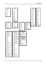
4-4-3 White Balance - Adjustment
3. W/B
(low light)
(hight light)
Sub Bright
R offset
G offset
B offset
Sub Contrast
R gain
G gain
B gain
(W/B adjustment Condition refer next page)
4-5. White Ratio (Balance) Adjustment
You can adjust the white ratio in factory mode (1:Calibration, 3:White-Balance).
Since the adjustment value and the data value vary depending on the input source, you have to
adjust these in CVBS, Component 1 and HDMI 1 modes.
The optimal values for each mode are configured by default. (Refer to Table 1, 2)
It varies with Panel’s size and Specification.
1.
2.
3.
- Equipment : CS-210
- Pattern: MIK K-7256 #92 “Flat W/B Pattern” as standard
- Use other equipment only after comparing the result with
that of the Master equipment.
- Set Aging time : 60min
- Calibration and Manual setting for WB adjustment.
HDMI : Time #6 720P, Pattern #24 Chessboard Calibration
Manual adjustment #92 pattern (720p)
COMP: Time #6 720P, Pattern #24 Chessboard Calibration
Manual adjustment at #92 pattern (720p)
CVBS: Time #2 PAL, Pattern #24 Chessboard Calibration
Manual adjustment at #92 pattern (NTSC)
PC: Time #21 1024*768, Pattern #24 Chessboard Calibration
Manual adjustment at #92 pattern (NTSC)
- If finishing in HDMI mode, adjustment coordinate is almost same in AV/COMP mode.
- White Balance Manual Adjustment
Summary of Contents for LE32A457C1D
Page 46: ...1 4 1 Precautions Memo ...
Page 55: ...7 1 7 Schematic Diagram 7 Schematic Diagram 7 1 Block Diagram ...
Page 56: ...7 2 7 Schematic Diagram 7 3 Schematic Diagrams for iDTV 7 3 1 MAIN POWER BLOCK ...
Page 57: ...7 3 7 Schematic Diagram 7 3 2 SOUND 7 3 3 HDMI ...
Page 58: ...7 4 7 Schematic Diagram 7 3 4 JACK INPUT TUNER 7 3 5 JACK_IN OUT 2 ...
Page 59: ...7 5 7 Schematic Diagram 7 3 6 SCALER 7 3 7 DDR SERVICE ...
Page 60: ...7 6 7 Schematic Diagram 7 3 8 FBE LVDS 7 3 9 EMMA ...
Page 61: ...7 7 7 Schematic Diagram 7 3 10 PCMCIA ...
Page 62: ...7 8 7 Schematic Diagram 7 3 11 DTV AUDIO ...
Page 63: ...7 9 7 Schematic Diagram 7 4 Schematic Diagrams for Ready 7 4 1 MAIN POWER BLOCK ...
Page 64: ...7 10 7 Schematic Diagram 7 4 2 SOUND 7 4 3 HDMI ...
Page 65: ...7 11 7 Schematic Diagram 7 4 4 JACK INPUT TUNER 7 4 5 JACK_IN OUT 2 ...
Page 66: ...7 12 7 Schematic Diagram 7 4 6 SCALER 7 4 7 DDR SERVICE ...
Page 67: ...7 13 7 Schematic Diagram 7 4 8 FBE LVDS ...
Page 68: ...7 14 7 Schematic Diagram Memo ...
Page 72: ...4 4 4 Troubleshooting WAVEFORMS 1 R G B Output Signal ...
Page 74: ...4 6 4 Troubleshooting WAVEFORMS 2 Digital Output Data 3 Signal of HDMI Data ...
Page 76: ...4 8 4 Troubleshooting WAVEFORMS 3 CVBS Output Signal 4 Tuner_CVBS Output Signal ...
Page 78: ...4 10 4 Troubleshooting WAVEFORMS 2 Digital Output Data 5 Analog Signal Y C ...
Page 96: ...4 28 4 Troubleshooting Memo ...
Page 100: ...6 4 6 Wiring Diagram 6 2 Wiring Picture 6 2 1 LE26 32 37A457C D 6 2 2 LE40A457C D ...
Page 101: ...6 5 6 Wiring Diagram 6 2 3 LE26 32 37A451C 6 2 4 LE40A451C ...
Page 104: ...6 8 6 Wiring Diagram Memo ...