Circuit Description
Samsung Electronics
13-11
■
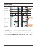
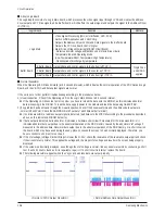
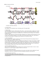
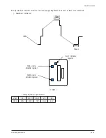
Drive Waveform Specifications
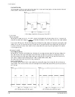
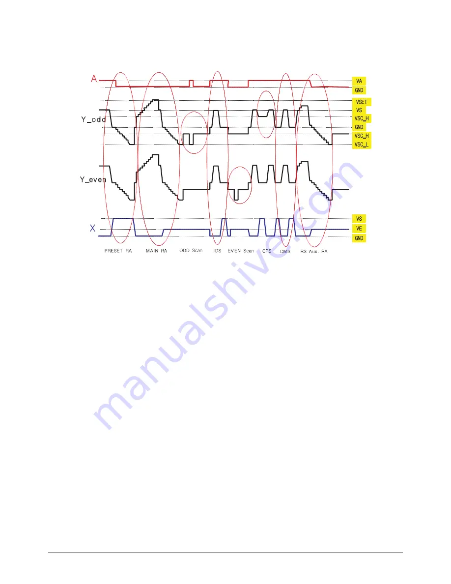
- Drive Waveform
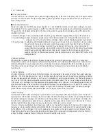
- Description of the function of each pulse
1) Y Preset RA Pulse
This is supplied to the first sub-field and erases the discharge status of the previous subfield.
2) Y Main RA Pulse
During the Y Rising Ramp section, approximately 300V~350V (Vscan-h + Vset) of external voltage is supplied to the Y electrode,
and a weak discharge is started when each gap voltage is equal to the discharge start voltage. While maintaining the weak dis-
charge, as a whole, negative wall charges are accumulated on the Y electrode and positive wall charges on the X electrode and
the address electrode.
During the Y Falling Ramp section, the negative wall charges accumulated on the Y electrode by the approximately 105V of X bias
are used to erase the positive wall charges on the X electrode, and the address electrode maintains most of the positive wall
charges accumulated during the (0V) Rising Ramp section preparing for the next address discharge.
3) Y Scan Pulse (Odd/Even)
A scan pulse classifies the Y electrode into Odd and Even lines and selects FPC output electrodes sequentially (one line-at-a-
time). At this time, Vscan is called the Scan Bias Voltage.
A Vscan voltage of approximately -175 Volt (Vsc_1) is supplied to the electrode lines. For the other lines, -56 volt (Vsc_h is higher
than Vscan-l by 120V) is supplied. However, negative wall charges are accumulated on the Y electrode by the Ramp pulse, and
positive wall charges are accumulated on the address electrode, and the voltage applied to the cells, to which the Address pulse
(70V~75V) has been applied, becomes higher than the discharge voltage. An address Discharge occurs as a result. Since the
Scan and Data pulse is applied one line at a time as above, the address time of PDP is very long.
4) IDS Pulse (InDependent Sustain Pulse)
Since an Odd Scan is performed first, the Odd line output sustains optical twice during the IDS section. At this time, a Sustain
Discharge does not occur for the Even line because the Even line is not scanned.
5) CPS Pulse (ComPare Sustain Pulse)
By floating the Odd line that caused the Sustain Discharge in the IDS section to the Vscan-h level, and introducing the Sustain
Discharge only for Even lines, it compensates for the optical output difference between the Even and Odd lines.
6) CMS Pulse (ComMon Sustain Pulse)
Actual optical is output during the common Sustain Discharge section.
Summary of Contents for HPS5033 - 50" Plasma TV
Page 11: ...1 6 Samsung Electronics MEMO ...
Page 47: ...3 30 Samsung Electronics MEMO ...
Page 50: ...Samsung Electronics 5 2 MEMO ...
Page 64: ...6 14 Samsung Electronics MEMO ...
Page 70: ...7 6 Samsung Electronics MEMO ...
Page 139: ...Circuit Description 13 18 Samsung Electronics Scan_l Even_Scan Y Sustain ...
Page 140: ...Circuit Description Samsung Electronics 13 19 Attachment 2 X Output Waveform X Sustain ...
Page 141: ...13 20 Samsung Electronics MEMO ...


