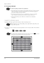
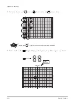
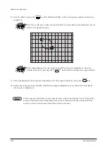
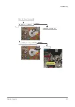
background image

Alignment and Adjustments

4-26

Samsung Electronics

Caution

Caution

ADD/DEL

SELF FOCUS

S.MODE

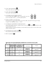
16.  Save the data by using the           key after the Red and Blue Color Convergence adjustment has been

completed.

The Cursor will move to the center and blink two times before it automatically moves
back to its original position.

After completing and saving  the R, G and B Convergence Adjustment , the data

should be saved by pressing the                   button before exiting Convergence Mode.

17.  After completing the Convergence Adjustment, exit Convergence Mode by using the             key.

18.  Follow the same procedure for DTV (1080i) Convergence Adjustment as you did for Normal Mode

Convergence Adjustment.

If Convergence Adjustment is not properly done, or the Convergence Center escaped the
sensor’s detection area, an adjustment error occurs. Therefore, the Jig Screen should be
used for precise Convergence Adjustment during servicing.

Note

Summary of Contents for HC-P4241W

Page 1: ...l HCP4241WX XAA HC P4241W PROJECTION TV RECEIVER CONTENTS Feature and Advantages Precautions Specifications Alignment and Adjustments Diagnostics Exploded View and Parts List Electric Parts List PCB Diagrams Schematic Diagrams 1 2 3 4 5 6 7 8 9 ...

Page 2: ...g Electronics Co Ltd MAR 2004 Printed in Korea AA82 01460A This Service Manual is a property of Samsung Electronics Co Ltd Any unauthorized use of Manual can be punished under applicable International and or domestic law ...

Page 3: ...ts metal cabinets screwheads and control shafts The current measured should not exceed 0 5 milliamp Reverse the power plug prongs in the AC outlet and repeat the test Fig 1 1 AC Leakage Test 6 Antenna Cold Check With the unit s AC plug disconnected from the AC source connect an electrical jumper across the two AC prongs Connect one lead of the ohmmeter to an AC prong Connect the other lead to the ...

Page 4: ...t appear to have overheated or that are otherwise damaged should be replaced with parts that meet the original specifications Always determine the cause of damage or overheat ing and correct any potential hazards 15 Observe the original lead dress especially near the following areas Antenna wiring sharp edges and especially the AC and high voltage power supplies Always inspect for pinched out of p...

Page 5: ... terminals and earphone jacks 6 Insulation Checking Procedure Disconnect the power cord from the AC source and turn the power switch ON Connect an insulation resistance meter 500V to the blades of the AC plug The insulation resistance between each blade of the AC plug and accessible conductive parts see above should be greater than 1 megohm 7 Never defeat any of the B voltage interlocks Do not app...

Page 6: ...oldering iron when soldering or unsoldering ESDs 6 Use only an anti static solder removal device Many solder removal devices are not rated as anti static these can accumulate sufficient electrical charge to damage ESDs 7 Do not remove a replacement ESD from its protective package until you are ready to install it Most replacement ESDs are packaged with leads that are electrically shorted together ...

Page 7: ...d Voltage W B Coordinates High Voltage FUSE Power Consumption Dimension Weight NTSC Progressive Scanning VHF CH2 CH13 75 ohm Unbalanced Video 45 75 MHz Sound 42 25 MHz Chrominance Subcarrier 42 17 MHz STD 10W MAX 15W 120V 60 Hz Hx 310 Hy 325 Y 11 Lx 300 Ly 295 Y 0 3 29KV 250V 6 3A CODE NO 3601 000300 240W 1004 X 471 X 967mm 39 5 X 18 5 X 38 0 inches 40 4Kg 89lbs ...

Page 8: ...MEMO 3 2 Samsung Electronics ...

Page 9: ...om starting screen will be selected 5 Any adjustable data changed will be automatically saved There is no separate Save key 4 1 2 Initial Display in Service Mode Deflection 480p offset 1080i offset Convergence NR Video Adjust 1 Video Adjust 2 Video Adjust 3 Video Adjust 4 Video Adjust DNIe Option CHECKSUM0000 Reset 4 1 3 Button Descriptions for Service Mode 1 When RF Patterns are Displayed MENU Fu...

Page 10: ... SC H Parabola Upper Corner Lower Corner H Trapezium Bow Angle V Position CXA Left Blk CXA Right Blk Initial Value 31 32 31 32 6 7 8 3 10 32 32 32 32 32 32 45 25 Range 0 63 0 63 0 63 0 63 0 63 0 63 0 63 0 63 0 63 0 63 0 63 0 63 0 63 0 63 0 63 0 63 0 63 EEP ROM Copy Data RF Mode 28 33 31 24 0 0 7 10 10 38 31 31 31 31 28 45 25 Remarks Adjustable Fixed Adjustable Fixed Fixed Fixed Fixed Fixed Fixed F...

Page 11: ...r H Trapezium Bow Angle V Position CXA Left Blk CXA Right Blk Initial Value 0 0 0 0 0 0 0 0 0 0 0 0 0 0 0 45 25 Range 63 63 63 63 63 63 63 63 15 15 15 15 15 15 15 15 63 63 63 63 63 63 63 63 63 63 63 63 63 63 63 63 63 63 480p Mode 0 0 0 0 0 0 0 0 0 0 0 0 0 0 0 45 25 Remarks Adjustable Adjustable Adjustable Adjustable Fixed Fixed Fixed Fixed Fixed Fixed Fixed Fixed Fixed Fixed Fixed Fixed Fixed Do n...

Page 12: ...r H Trapezium Bow Angle V Position CXA Left Blk CXA Right Blk Initial Value 0 0 0 0 0 0 0 0 0 0 0 0 0 0 0 50 25 Range 63 63 63 63 63 63 63 63 15 15 15 15 15 15 15 15 63 63 63 63 63 63 63 63 63 63 63 63 63 63 63 63 63 63 1080i Mode 0 0 0 0 0 0 0 0 0 0 0 0 0 0 1 50 25 Remarks Adjustable Adjustable Adjustable Adjustable Fixed Fixed Fixed Fixed Fixed Fixed Fixed Fixed Fixed Fixed Fixed Fixed Fixed Do ...

Page 13: ...e NR Low Value NR Hight Ref s NR Low Ref s NR Hight Value s NR Low Value s NR Read M S Initial Value 0 15 0 15 15 0 15 40 3 17 51 20 0 17 50 Range 0 1 63 63 63 63 63 63 63 63 63 63 63 63 0 127 0 127 128 127 128 127 0 127 0 127 128 127 128 127 RF 0 5 0 0 5 0 5 40 3 17 51 17 0 17 50 Remarks Fixed Fixed Fixed Fixed Fixed Fixed Fixed Fixed Fixed Fixed Fixed Fixed Fixed Fixed Fixed Read Price Do not ch...

Page 14: ...5 7 16 8 1 1 2 207 111 211 Remarks Adjustable Fixed Adjustable Fixed Adjustable Adjustable Adjustable Fixed Adjustable Adjustable Adjustable Fixed Fixed Fixed Fixed Fixed Fixed Fixed Fixed Video Adjust 1 RF 1080i is Separated R Cutoff G Cutoff B Cutoff COLOR On Off CR Offset CB Offset R Drive G Drive B Drive Sub Bright Sub Contrast Sub Color Sub Tint CTI Level COL AXIS LTI Level 9405 U OUT 9405 Y ...

Page 15: ...4 5 6 7 8 9 10 11 12 13 14 15 16 17 18 Initial Value 3 2 3 2 15 2 0 0 0 0 1 0 11 13 30 30 2 3 Range 0 3 0 3 0 3 0 3 0 15 0 3 0 3 0 3 0 3 0 3 0 3 0 1 0 15 0 31 0 31 0 31 0 7 0 7 1080i 3 1 2 2 15 3 0 1 0 1 480p 1 1 13 16 31 30 1 2 ALL mode Except 1080i 3 1 3 3 15 ALL mode 3 ALL mode 0 0 0 3 Except 480p 1 ALL mode 0 13 ALL mode 16 31 30 1 2 Remarks Fixed Fixed Fixed Fixed Fixed Fixed Fixed Fixed Fixe...

Page 16: ...Volume Video Mute Time S ABL P_ABL PLIMT_LEV AKB CLP Gate Color Kil Real Time Hour Initial Value 10 16 0 0 0 0 0 5 2 4 500ms 0 0 0 0 1 198 72 Range 16 127 16 127 0 15 0 15 0 7 0 7 0 1 0 9 0 15 0 20 0 1sec 0 3 0 2 0 2 0 1 0 1 0 255 0 255 ALL mode 10 16 1 8 0 1 0 0 2 4 500ms 0 0 0 0 1 198 72 Remarks Fixed Fixed Fixed Fixed Fixed Fixed Fixed Fixed Fixed Fixed Fixed Fixed Fixed Fixed Fixed Fixed Fixed...

Page 17: ...lay_480p 1E Data1 9405 1E Data2 9405 1E Data3 9405 Initial Value 1 1 1 1 5 1 28 28 30 28 2 4 5 4 1 15 15 14 Range 0 3 0 3 0 3 0 3 0 1 0 7 0 7 0 63 0 63 0 63 0 63 0 7 0 7 0 7 0 3 0 15 0 15 0 15 Only Indicated Mode 1 1 1 1 3 1 28 28 30 28 2 4 5 4 1 15 15 14 Remarks 2 Fixed Fixed Fixed Fixed Fixed Fixed Fixed Fixed Fixed Fixed Fixed Fixed Fixed Fixed Fixed Fixed Fixed Fixed Remarks 1 RF VSD AV SV DVD...

Page 18: ...Gain DEP TH Cor DEP OV Gain H DEP R INT CTE Gain Initial Value 0 0 0 0 0 0 0 0 0 0 0 0 0 0 0 0 1080i 0 0 0 0 0 0 0 0 0 0 0 0 0 0 0 0 Remarks Fixed Fixed Fixed Fixed Fixed Fixed Fixed Fixed Fixed Fixed Fixed Fixed Fixed Fixed Fixed Fixed Range 0 127 0 127 0 127 0 255 0 255 0 3 0 255 0 255 0 255 0 255 0 255 0 15 0 63 0 255 0 127 0 255 RF 0 0 0 0 0 0 0 0 0 0 0 0 0 0 0 0 AV SV 480i 480p 0 0 0 0 0 0 0 ...

Page 19: ...ct Burst Screen LNA Initial Value 4 3 On Off On On On CT Off On On USA Off On Off Off Off Off Range Wide 4 3 On Off On Off On Off On Off On Off CT EN SP FR CT A EN SP FR On Off On Off On Off USA On Off On Off On Off On Off On Off On Off Mexico South Central America 42 47 52 Wide Off Off On On On CT EN SP FR Off Off Off USA Off On Off Off Off On North America 42 47 52 Wide Off Off On On On CT EN SP...

Page 20: ...gnment and Adjustments 4 12 Samsung Electronics 4 3 Screen Change When adjusting I2 C Bus Geometric items 8 H Trapezium 10 BOW 5 ANGLE 4 H Parabola 2 V LINEARITY 6 V SIZE 3 H SIZE 9 H SHIFT 7 VSC 1 V SHIFT ...

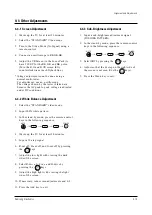
Page 21: ... STANDARD video mode 2 Input 100 white pattern 3 In the stand by mode press the remote control keys in the following sequence 4 Warm up the TV for at least 30 minutes 5 Input a 10 step signal 6 R cut off B cut off and G cut off by pressing the keys 7 Adjust the low light with viewing the dark side of the screen 8 Select R drive G drive and B drive by pressing the keys 9 Adjust the high light with ...

Page 22: ... Set the pattern to Crosshatch Adjust the electric focus before beginning Adjust the DY tilt TILT before beginning 2 How to Adjust Green Lens Adjustment Loosen the lens screw for easier adjustment Press Mute 1 8 and 3 sequentially to enter Convergence Mode Display only the Green pattern by using the 100 0 and Previous Channel Keys in order to turn the R G and B patterns On Off respectively Turn th...

Page 23: ...ny light around the core disappears 11 Adjust G Focus so that the surrounding flash can disappear from the spot 12 After G Focus adjustments are complete adjust R Focus as above procedures 13 The B CRT adjustments can be omitted because the variance of beam focus is small Only Vm coil is mounted 14 Adjust the Focus pack VR for fine focusing 15 Press the button on the remote control and the mode ch...

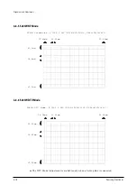
Page 24: ... 2 30 12 Y 440 28 2 64 6 4241W 4241W Screen Size X 925 Y 523 X 396 12 2 31 12 Y 488 40 2 68 6 22 02mm 73 41mm 33 28mm 76 07mm 22 02mm 33 28mm 28 03mm 72 41mm 42 87mm 72 88mm 28 03mm 42 87mm 4 6 1 4241W RF Mode 4 6 2 4241W DTV Mode The DTV Mode Adjustment is available only when a Set top Box is connected ...

Page 25: ...2 Y 440 28 2 64 6 474 474 1W DTV M ode X 1045 Y 588 X 396 12 2 31 12 Y 488 40 2 68 6 24 88mm 82 94mm 37 42mm 85 53mm 24 88mm 37 42mm 31 67mm 81 81mm 48 20mm 81 93mm 31 67mm 48 20mm 4 6 3 4741W RF Mode 4 6 4 4741W DTV Mode The DTV Mode Adjustment is available only when a Set top Box is connected ...

Page 26: ... 12 Y 440 28 2 64 6 524 524 1W DTV M ode X 1153 Y 649 X 396 12 2 31 12 Y 488 40 2 68 6 27 45mm 91 51mm 41 3mm 94 4mm 27 45mm 41 3mm 34 94mm 90 26mm 53 20mm 90 43mm 34 94mm 53 20mm 4 6 5 5241W RF Mode 4 6 6 5241W DTV Mode The DTV Mode Adjustment is available only when a Set top Box is connected ...

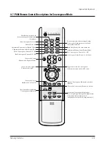
Page 27: ...rds Right or Down Recalls the previous data before convergence adjustment Initializes Sets Convergence Data to 0 Normal Line shif Adjustment Pattern Select Button Green Adjustment Pattern Select Button Red Green Convergence Pattern ON OFF Red Convergence Pattern ON OFF Save data after completing Convergence Adjustment Automatic Convergence Adjustment after completing Convergence Adjustments Automa...

Page 28: ...ignal Allows for comparison between the Adjustment screen and the Normal screen during adjusment Each press of the key will switch between modes 9 LINE SHIFT KEY Repeat Fine Adjustment no indication Line Adjustment Enter Mode This key selects between line or movement whole pattern movement or individual quadrant movement up down left right at the beginning of the Convergence Adjustment Press the k...

Page 29: ...ng the Convergence Adjustment pattern in the left or right direction in order to fit the center of the screen Before beginning Convergence Adjustment precisely match the center of the TV screen with the center of the Convergence screen 18 CONVERGENCE DATA ZERO KEY Press to zero the convergence correction data 19 FINE COARSE KEY Changes when applying Almighty Cg Module How to extract the basic Cg D...

Page 30: ...rea Sensors are on the center of each of the 4 faces 3 Adjustment should be precise otherwise an Automatic Color Adjustment error occurs 1 Aging the TV over 30 minutes is required 2 Apply the NTSC input signal from the antenna or other external input source Before adjusting the Green Red and Blue patterns adjust the DY of the CRT to avoid having a tilted center line 3 Press Mute 1 8 and 3 on the r...

Page 31: ...SELECT to adjust the Green Color Convergence first For the first entrance Green Color Convergence will automatically be selected 5 Press the key to move the cursor right the button to move the cursor left 6 Scene Adjustment Use the left œ right up down buttons to move the cursor and use the channel button and the volume buttons to adjust the convergence ...

Page 32: ...rtical moves select and press to move down and to move down Pressing the key again will switch to horizontal movement 8 Use the Line Move Key for global shaping in the beginning stages of Convergence Adjustment Alignment and Adjustments 4 24 Samsung Electronics ...

Page 33: ...Press the button to release the Red Color from mute and select the Red Color by pressing the key 12 Perform steps 5 10 to adjust the Red Color Convergence 13 Adjust the Blue Color based on the Green Color Press the button to mute the Red Color again Release the Blue Color from mute by pressing and select the Blue Color by pressing the key 14 Adjust the Blue Color Convergence by performing steps 5 ...

Page 34: ...R G and B Convergence Adjustment the data should be saved by pressing the button before exiting Convergence Mode 17 After completing the Convergence Adjustment exit Convergence Mode by using the key 18 Follow the same procedure for DTV 1080i Convergence Adjustment as you did for Normal Mode Convergence Adjustment If Convergence Adjustment is not properly done or the Convergence Center escaped the ...

Page 35: ...0 245 150 4 7 3 Self Focus Convergence Mode 1 After completing the Convergence Adjustment press the Memory button to save the data and exit back to a black screen Then enter Convergence Mode again to do the Automatic Color Adjustment by pressing the Automatic Color Adjustment button ADD DEL ...

Page 36: ...Convergence Module CNZ01 PIN NAME PIN NAME 1 N C 17 GND 2 GND 18 GND 3 D FOCUS 19 BV 4 GND 20 BH 5 D2 SCL 21 GV 6 D1 22 GH 7 GND 23 RV 8 C SYNC 24 RH 9 CG R 25 GND 10 CG G 26 H BLK 11 CG B 27 V BLK 12 D3 SDA 28 GND 13 N C 29 N C 14 IR 30 5V 15 F BLK 31 5V CG 16 GND 32 GND ...

Page 37: ...iagnostics 5 1 Opening the Set and Replacing Assemblies 5 1 1 Replacing and Repairing Each Assembly Opening the Back Cover Remove all indicated screws on the rear side of the Set Repair or replace the required Assembly MAIN DY JACK SUB CG Module ...

Page 38: ... CRT PCB Opening the Front Cover Troubleshooting 5 2 Samsung Electronics Remove all indicated screws and open the Front Cover Repair the frontal PCB CRT or replace it after removing the attached connectors PCB CRT R PCB CRT G PCB CRT B ...

Page 39: ...k Cover Remove the screws indicated and detach the Top Cover Remove the Dust Cover that prevents dust from entering into the screen Before proceeding disconnect all the DY and Connectors connected to the assembly Remove the 4 corner screws from the CRT and replace the CRT 5 1 3 Replacing a Burnt or Exhausted CRT ...

Page 40: ...utput voltages and waveforms of CN801 and CN802 on the SUB Board Normal Normal Abnormal Abnormal Check the output terminal of CNZ02 BV BH RV RH GV GH Check the respective circuits regarding the symptoms Replace the Convergence Module Validate the H BLK and V BLK outputs of the MAIN Board ...

Page 41: ...bnormal Abnormal Abnormal Check IC601 Output Terminal Pins 2 and 4 Insert the CN601 Connector Check the Speakers Check IC601 Input Terminal Pin 3 Check FD802S of the SUB Board Check IC601 Input Terminal Pin 5 Check the Sound Mute Circuit Check IC601 Input Terminal Pins 7 and 11 Check IC601 Check IC602 Check IC602 Input Terminals Check IC605 Input Terminals ...

Page 42: ...ound Normal Normal Normal Normal Normal Abnormal Abnormal Abnormal Check the Heater Check for High Voltage Check CN501 Pins 1 3 and 5 Check IC501 531 and 561 Check the CN501 Connector Replace the CN501 Connector Check IC04 Input Terminal Pins 20 21 and 22 Check IC03 Check IC04 ...

Page 43: ...Troubleshooting Samsung Electronics 5 7 Normal Abnormal Abnormal Check the Heater Abnormal Replace R513 543 and 573 Check CB504 Pin 5 of the CRT PCB Replace R513 543 and 573 Check R464 ...

Page 44: ...MEMO 5 8 Samsung Electronics ...

Page 45: ...Q2 HIPS V0 GR503 1 T0103 BP59 00045A MODULE FOCUS PACK ASS Y SVP 43W6HE F301 1 T0115 AA61 00475B BRACKET CRT MAIN 54 SECC T1 6 1 T0601 BP91 00992A ASSY PRT 42Q2 P59A 1 S N A T0137 BP94 00659A ASSY PCB MISC LINE FILTER HCP4241WX XAA 1 S N A T0073 BP94 00771A ASSY PCB MAIN HCP4241WX XAA P60A 1 T0097 BP94 02114A ASSY PCB MISC PWR DEF HCP4241WX XAA P60A 1 S N A T0095 BP64 00408A CABINET BACK BOTTOM 42...

Page 46: ...AA60 40014A PIN GT ASSY AUTO S N A 4 GT812 AA60 40014A PIN GT ASSY AUTO S N A 4 GT813 AA60 40014A PIN GT ASSY AUTO S N A 4 GT814 AA60 40014A PIN GT ASSY AUTO S N A 4 OO BP41 00052A PCB LINE FILTER 42Q2 L FILTER 1L 1 6T 24 S N A 2 T0073 BP94 00771A ASSY PCB MAIN HCP4241WX XAA P60A 3 0202 001366 SOLDER WIRE FLUX RS60S D1 2 63Sn 37Pb S N A 3 IC902 1102 001130 IC EPROM M27W201 80F6 256KX8BIT DIP 32P 3...

Page 47: ...2007 000084 R CHIP 4 7Kohm 5 1 10W TP 1608 5 RO87 2007 000084 R CHIP 4 7Kohm 5 1 10W TP 1608 5 RO87 2007 000084 R CHIP 4 7Kohm 5 1 10W TP 1608 5 RO87 2007 000084 R CHIP 4 7Kohm 5 1 10W TP 1608 5 RO87 2007 000084 R CHIP 4 7Kohm 5 1 10W TP 1608 5 RO87 2007 000084 R CHIP 4 7Kohm 5 1 10W TP 1608 5 RO87 2007 000084 R CHIP 4 7Kohm 5 1 10W TP 1608 5 RO87 2007 000084 R CHIP 4 7Kohm 5 1 10W TP 1608 5 RO87 ...

Page 48: ...R 4 2 1 6T 220 235 1 S N A 5 RO87 2007 000082 R CHIP 3 3Kohm 5 1 10W TP 1608 5 RO87 2007 000082 R CHIP 3 3Kohm 5 1 10W TP 1608 5 RO87 2007 000082 R CHIP 3 3Kohm 5 1 10W TP 1608 5 0202 001376 SOLDER CREAM RX3603 2330HO S45A PASTE Sn S N A 3 MIC801 BP96 00335E ASSY HEAT SINK P BP62 00035A SCREW SLA30 S N A 4 H S 0205 001154 OIL SILICON G746 S N A 4 IC012 1203 000203 IC POSI ADJUST REG 3050 TO 220 5P...

Page 49: ...T 5 T0156 0501 000344 TR SMALL SIGNAL KSC1623 G NPN 200mW SOT 5 T0156 0501 000344 TR SMALL SIGNAL KSC1623 G NPN 200mW SOT 5 T0156 0501 000344 TR SMALL SIGNAL KSC1623 G NPN 200mW SOT 5 T0156 0501 000344 TR SMALL SIGNAL KSC1623 G NPN 200mW SOT 5 T0156 0501 000344 TR SMALL SIGNAL KSC1623 G NPN 200mW SOT 5 T0156 0501 000344 TR SMALL SIGNAL KSC1623 G NPN 200mW SOT 5 T0156 0501 000344 TR SMALL SIGNAL KS...

Page 50: ...074 R CHIP 100ohm 5 1 10W TP 1608 5 RO87 2007 000074 R CHIP 100ohm 5 1 10W TP 1608 5 RO87 2007 000074 R CHIP 100ohm 5 1 10W TP 1608 5 RO87 2007 000074 R CHIP 100ohm 5 1 10W TP 1608 5 RO87 2007 000074 R CHIP 100ohm 5 1 10W TP 1608 5 RO87 2007 000074 R CHIP 100ohm 5 1 10W TP 1608 5 RO87 2007 000074 R CHIP 100ohm 5 1 10W TP 1608 5 RO87 2007 000074 R CHIP 100ohm 5 1 10W TP 1608 5 RO87 2007 000074 R CH...

Page 51: ...1167 R CHIP 75ohm 5 1 10W TP 1608 5 RO87 2007 007651 R CHIP 9 1Kohm 1 1 10W TP 1608 5 T0657 2203 000181 C CER CHIP 100nF 80 20 25V Y5V TP 2012 5 T0657 2203 000181 C CER CHIP 100nF 80 20 25V Y5V TP 2012 5 T0657 2203 000181 C CER CHIP 100nF 80 20 25V Y5V TP 2012 5 T0657 2203 000181 C CER CHIP 100nF 80 20 25V Y5V TP 2012 5 T0657 2203 000181 C CER CHIP 100nF 80 20 25V Y5V TP 2012 5 T0657 2203 000181 C...

Page 52: ... C CER CHIP 47nF 10 25V X7R TP 1608 5 T0657 2203 000975 C CER CHIP 47nF 10 25V X7R TP 1608 5 T0657 2203 000975 C CER CHIP 47nF 10 25V X7R TP 1608 5 T0657 2203 000975 C CER CHIP 47nF 10 25V X7R TP 1608 5 T0657 2203 000975 C CER CHIP 47nF 10 25V X7R TP 1608 5 T0657 2203 000975 C CER CHIP 47nF 10 25V X7R TP 1608 5 T0657 2203 000975 C CER CHIP 47nF 10 25V X7R TP 1608 5 T0657 2203 000998 C CER CHIP 0 0...

Page 53: ... AL CHIP 47UF 20 50V GP TP 6 3X7 7MM 5 C653 2402 001145 C AL CHIP 47UF 20 50V GP TP 6 3X7 7MM 5 C656 2402 001145 C AL CHIP 47UF 20 50V GP TP 6 3X7 7MM 5 C662 2402 001145 C AL CHIP 47UF 20 50V GP TP 6 3X7 7MM 5 C706 2402 001145 C AL CHIP 47UF 20 50V GP TP 6 3X7 7MM 5 C741 2402 001145 C AL CHIP 47UF 20 50V GP TP 6 3X7 7MM 5 C742 2402 001145 C AL CHIP 47UF 20 50V GP TP 6 3X7 7MM 5 MC813 2402 001145 C...

Page 54: ... HEADER BOX 11P 1R 2 5MM ANGLE S N A 3 T0081 6003 001023 SCREW TAPTITE RWH B M3 L10 ZPC YEL SW S N A 3 BP97 00600A ASSY AUTO SVP 42W5HL P59A CHAMP 4 R125 2001 000429 R CARBON 1KOHM 5 1 8W AA TP 1 8X3 2MM 4 R125 2001 000832 R CARBON 510OHM 5 1 8W AA TP 1 8X3 2MM 4 R125 2001 000832 R CARBON 510OHM 5 1 8W AA TP 1 8X3 2MM 4 R125 2001 000832 R CARBON 510OHM 5 1 8W AA TP 1 8X3 2MM 4 R125 2001 000924 R C...

Page 55: ...ZP7 5B 7 5 8 4V 1000MW DO 4 4 DZ016 0403 000708 DIODE ZENER MTZJ13B 12 59 13 16V 500MW D 4 DZ016 0403 000708 DIODE ZENER MTZJ13B 12 59 13 16V 500MW D 4 DZ016 0403 000716 DIODE ZENER MTZJ4 7B 4 59 4 77V 500MW DO 4 DZ016 0403 000719 DIODE ZENER MTZJ7 5B 7 11 7 44V 500MW DO 4 DZ016 0403 000734 DIODE ZENER TZP15B 14 7 16 5V 1000MW DO 4 DZ016 0403 000734 DIODE ZENER TZP15B 14 7 16 5V 1000MW DO 4 DZ016 ...

Page 56: ... 15Kohm 5 3W AA TP 6x16 4 R418 2003 000540 R METAL OXIDE S 1Kohm 5 2W AF TP 4x12m 4 R419 2003 000540 R METAL OXIDE S 1Kohm 5 2W AF TP 4x12m 4 R425 2003 000586 R METAL OXIDE S 22Kohm 5 2W AF TP 4x12 4 R426 2003 000586 R METAL OXIDE S 22Kohm 5 2W AF TP 4x12 4 R318 2003 000690 R METAL OXIDE S 4 7ohm 5 2W AA TP 4x12 4 R303 2003 001018 R METAL OXIDE S 220ohm 5 2W AF TP 3 9x 4 R420 2003 001018 R METAL O...

Page 57: ... 2401 000010 C AL 220uF 20 16V GP 6 3x11mm 2 4 C701 2401 000025 C AL 100uF 20 16V GP TP 6 3x11 5 4 C701 2401 000050 C AL 10uF 20 16V GP TP 5x11 2 5 4 C701 2401 000142 C AL 1000uF 20 16V WT TP 10x20 5 4 C701 2401 000215 C AL 0 1UF 20 50V GP TP 4X7MM 5 4 C701 2401 000302 C AL 100uF 20 25V GP TP 6 3x11 5 4 C701 2401 000302 C AL 100uF 20 25V GP TP 6 3x11 5 4 C701 2401 000302 C AL 100uF 20 25V GP TP 6 ...

Page 58: ...YELET ID1 5 OD2 L2 8 NI SN BSP3 1 2H S N A 4 EY79 6042 000002 EYELET ID1 5 OD2 L2 8 NI SN BSP3 1 2H S N A 4 EY8 6042 000002 EYELET ID1 5 OD2 L2 8 NI SN BSP3 1 2H S N A 4 EY80 6042 000002 EYELET ID1 5 OD2 L2 8 NI SN BSP3 1 2H S N A 4 EY81 6042 000002 EYELET ID1 5 OD2 L2 8 NI SN BSP3 1 2H S N A 4 EY85 6042 000002 EYELET ID1 5 OD2 L2 8 NI SN BSP3 1 2H S N A 4 EY86 6042 000002 EYELET ID1 5 OD2 L2 8 NI...

Page 59: ...2001 000429 R CARBON 1KOHM 5 1 8W AA TP 1 8X3 2MM 4 R125 2001 000472 R CARBON 2 7KOHM 5 1 8W AA TP 1 8X3 2MM 4 R125 2001 000539 R CARBON 24KOHM 5 1 8W AA TP 1 8X3 2MM 4 R125 2001 000563 R CARBON 27KOHM 5 1 8W AA TP 1 8X3 2MM 4 R125 2001 000577 R CARBON 2KOHM 5 1 8W AA TP 1 8X3 2MM 4 R125 2001 000613 R CARBON 3 9KOHM 5 1 8W AA TP 1 8X3 2MM 4 R125 2001 000734 R CARBON 4 7KOHM 5 1 8W AA TP 1 8X3 2MM ...

Page 60: ... BRACKET SCREEN TB 42W5 SECC T1 0 S N A 3 T0559 BP61 00043B HOLDER SENSOR W9 PC HB VIOLET S N A 3 BP61 00052A HOLDER WIRE PJTV NYLON 66 NATURAL S N A 2 BP61 00024E BRACKET SCREEN ASSY BOT 42W5 SECC T1 0 S N A 3 T0069 AA60 00091J SPACER FELT FELT 330X10 BLK T0 5 S N A 3 AA65 00020A CLAMPER CORE WIRE 55W9 NYLON 66 S N A 3 T0559 BP61 00043B HOLDER SENSOR W9 PC HB VIOLET S N A 3 BP61 00052A HOLDER WIR...

Page 61: ...PACER CRT PROJ 65 SILICONE D GRAY S N A 3 T0081 AA60 10011A SCREW TAPTITE SWRCH18A M4 L12 HH PC S N A 3 AA61 00056B BRACKET LENS PROJECTION SECC T1 6 S N A 3 AA61 00808B CASE COUPLER B PROJ ALDC T8 BLK S N A 3 T0114 AA61 00810B HOLDER CAP PROJ PC CLR S N A 3 T0511 AA63 00076B SPACER LENS FELT W7 BLK T0 8 S N A 3 T0107 AA91 00722A ASSY BRKT CRT SECC T1 6 PROJ S N A 4 T0072 AA61 00473B BRACKET CRT 5...

Page 62: ...Samsung Electronics Wiring Diagrams 8 1 8 1 MAIN PCB 8 PCB Diagram ...

Page 63: ...8 2 SUB PCB Wiring Diagrams 8 2 Samsung Electronics ...

Page 64: ...9 Schematic Diagrams Samsung Electronics Schematic Diagrams 9 1 9 1 MAIN 1 This Document can not be used without Samsung s authorization ...

Page 65: ...Schematic Diagrams 9 2 Samsung Electronics TP01 TP02 9 2 MAIN 2 TP01 TP02 This Document can not be used without Samsung s authorization ...

Page 66: ...Samsung Electronics Schematic Diagrams 9 3 9 3 MAIN 3 TP03 TP04 TP03 TP04 This Document can not be used without Samsung s authorization ...

Page 67: ...ung Electronics 9 4 MAIN 4 TP18 TP17 TP16 TP15 TP14 TP13 TP12 TP11 TP10 TP09 TP07 TP08 TP06 TP05 TP05 TP06 TP07 TP08 TP09 TP10 TP11 TP12 TP13 TP14 TP15 TP16 TP17 This Document can not be used without Samsung s authorization TP18 ...

Page 68: ...Samsung Electronics Schematic Diagrams 9 5 9 5 MAIN 5 This Document can not be used without Samsung s authorization ...

Page 69: ...Schematic Diagrams 9 6 Samsung Electronics 9 6 MAIN 6 This Document can not be used without Samsung s authorization ...

Page 70: ...Samsung Electronics Schematic Diagrams 9 7 9 7 SUB 1 TP19 21V TP19 This Document can not be used without Samsung s authorization ...

Page 71: ...Schematic Diagrams 9 8 Samsung Electronics 9 8 SUB 2 This Document can not be used without Samsung s authorization ...

Page 72: ...Samsung Electronics Schematic Diagrams 9 9 9 9 SUB 3 TP20 TP21 This Document can not be used without Samsung s authorization TP20 TP21 ...

Page 73: ...Schematic Diagrams 9 10 Samsung Electronics 9 10 SUB 4 This Document can not be used without Samsung s authorization ...

Page 74: ...Samsung Electronics Schematic Diagrams 9 11 9 11 CG MDL 1 This Document can not be used without Samsung s authorization ...

Page 75: ...Schematic Diagrams 9 12 Samsung Electronics 9 12 CG MDL 2 This Document can not be used without Samsung s authorization ...

Page 76: ...Samsung Electronics Schematic Diagrams 9 13 9 13 CRT This Document can not be used without Samsung s authorization ...

Page 77: ...Schematic Diagrams 9 14 Samsung Electronics 9 14 VM SIDE A V This Document can not be used without Samsung s authorization SIDE A V VM ...

Page 78: ...9 15 KEY CONTROL POWER CONTROL Samsung Electronics Schematic Diagrams 9 15 POWER CONTROL This Document can not be used without Samsung s authorization KEY CONTROL ...

Reviews: