


SAMSUNG Proprietary-Contents may change without notice
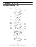
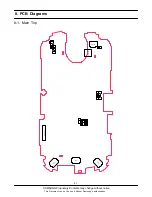
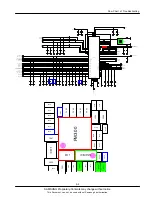
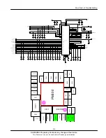
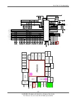
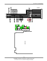
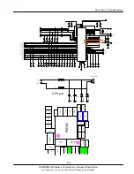
8. PCB Diagrams
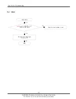
8-1
This Document can not be used without Samsung's authorization
8-1. Main Top
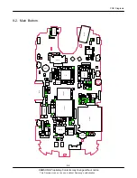
0
0
2
C
1
0
2
C
4
0
2
C
C2
05
C206
7
0
2
C
C2
16
9
1
2
C
0
2
2
C
1
2
2
C
3
2
2
C
4
2
2
C
0
3
2
C
C413
C4
29
0
4
4
C
1
4
4
C
C4
42
3
4
4
C
C4
49
C4
50
C4
51
2
5
4
C
CL
R
5
0
4
D
6
0
4
D
D
N
E
F4
04
HD
C4
02
0
0
2
L
1
0
2
L
2
0
2
L
4
1
4
L
5
1
4
L
6
1
4
L
L417
D
A
P
_
G
A
T
J
_
R
E
T
S
A
M
0
2
2
R
1
0
4
R
R4
05
R412
3
1
4
R
0
0
3
D
A
P
V
C
R
D
N
E
S
U4
01


