background image

6  Reference Information 

6-6 

SAM4S ER-380M/F SERIES


6-1 Semiconductor Base Diagram 

6-1-4 Other ICs 


Figure 6-11 SSCG FS781 Specification


Figure 6-12 VFD Driver UDN5812 Specification 

4

5

6

7

8

9

10

19

20

21

22

23

24

25

LOAD

SUPPLY

BB

V

OUT

2

OUT

7

OUT

8

OUT

19

OUT

18

OUT

13

12

13

14

27

28

17

18

SERIAL

DATA O UT

BLANKING

LOGIC
SUPPLY

STROBE

GROUND

CLOCK

CLK

ST

BLNK

OUT

9

OUT

10

OUT

12

OUT

11

11

LAT

CH

ES

R

EGISTE

R

R

EGISTE

R

LAT

CH

ES

2

3

2

6

27

28

SERIAL
DATA I N

OUT

6

OUT

1

OUT

4

OUT

3

OUT

20

1

15

16

OUT

5

OUT

17

OUT

16

OUT

15

OUT

14

DD

V


MOS

BIPOLAR

OUT

1

OUT

2

GROUND

D

wg. FP -013-1

OUT

3

OUT

N

CLOCK

SERIAL

DATA I N

STROBE

BLANKING

SERIAL
DATA O UT

SERIAL-PARALLEL S HIFT  REGISTER


LATCHES      

V

DD

V

BB

LOGIC
SUPPLY

LOAD
SUPPLY

Refer to page 12 for package dimensions.

Pin Description

Pin No.

Pin Name

I/O

TYPE

Description

1/2

Xin / Xout

I/O

Analog

Pins form an on-chip reference oscillator when connected to
terminals of an external parallel resonant crystal.  Xin may be
connected to TTL/CMOS external clock source.  If  Xin
connected to external clock other than crystal, leave Xout (pin 2)
unconnected.

7/3

S0 / S1

I

CMOS/TTL

Digital control inputs to select input frequency range and output
frequency scaling. Refer to Tables 7 & 8 for selection. S0 has
internal pulldown. S1 has internal pullup.

4

LF

I

Analog

Loop Filter. Single ended tri-state output of the phase detector.  A
two-pole passive loop filter is connected to Loop Filter (LF).

6

FSOUT

O

CMOS/TTL

Modulated Clock Frequency Output. The center frequency is the
same as the input reference frequency for FS781. Input
frequency is multiplied by 2x and 4x for FS782 and FS784
respectively.

8

VDD

P

Power

Positive Power Supply.

5

VSS

P

Power

Power Supply Ground

Table 1

Output Frequency Selection

Product Number

FSOUT Frequency Scaling

Description

FS781

1x

1x Modulated Frequency of Input Clock

FS782

2x

2x Modulated Frequency of Input Clock

FS784

4x

4x Modulated Frequency of Input Clock

Table 2. FSOUT SSCG (Modulated Output Clock) Product Selection

1

2

3

4

8

7

6

5

S0

VDD

Xin

Xout

FSOUT

VSS

LF

S1

FS78x

8 Pin TSSOP Package

1

2

3

4

8

7

6

5

Xin

Xout

S1

LF

VDD

S0

FSOUT

VSS

FS78x

8 Pin SOIC Package

Summary of Contents for ER-380F

Page 1: ...ecifications 3 Installation and Operation 4 Disassembly and Assembly 5 Maintenance and Adjustment 6 Reference Information 7 Special Circuit Descriptions 8 Troubleshooting 9 Exploded Views and Parts List 10 PCB Layout and Parts List 11 Block diagram 12 Wiring Diagram 13 Schematic Diagrams SERVICE ER 380M EL EC TR ON I CA SH R EGI ST ER ...

Page 2: ......

Page 3: ...es Electronic Cash Register Notes Notes may appear anywhere in the manual They describe additional information about the item Precaution symbols Indicates a Safety Precaution that applies to this part component Indicates the part or component is an electro statically sensitive device Use caution when handling these parts ...

Page 4: ...al may not in whole or in part be copied photocopied reproduced translated or converted to any electronic or machine readable from without prior written permission of Shin Heung Precision SAM4S ER 380M F SERIES Service Manual First edition JAN 2004 V1 0 Printed in KOREA ...

Page 5: ...ooting All information in this manual is subject to change without prior notice Therefore you must check the correspondence of your manual with your machine No part of this manual may be copied or reproduced in any form or by any means without the prior written consent of Shin Heung Precision Note Before using this Electronic Cash Register SECR for the first time leave it powered on in the REG mod...

Page 6: ...edges and especially the AC and high voltage supplies Always inspect for pinched out of place or frayed wiring Do not change the spacing between comp onents and the printed circuit board Check the AC power cord for damage Make sure that leads and components do not touch thermally hot parts 7 Product Safety Notice Some electrical and mechanical parts have special safety related characteristics whic...

Page 7: ...instrument s ground lead to the instrument chassis ground before connecting the positive lead always remove the instrument s ground lead last 1 3 Precautions for Electrostatic Sensitive Devices ESDs 1 Some semiconductor solid state devices are easily damaged by static electricity Such components are called Electrostatic Sensitive Devices ESDs examples include integrated circuits and some field eff...

Page 8: ...charged Interface Serial RS 232C Flow Control DTR DSR H W Flow Control XON XOFF S W Flow Control Baud Rate 1200 2400 4800 9600 19200 Bps Connector DB9P Female I F PBA Voltage Supply VCC 5V 200mA supplies at 9Pin of Connector RS 232C 1 RS 232C 2 Printer Model Shin Heung STM 210 Printing Speed 50 mm Sec 13 3 Line Sec Paper Dimension 57 5mm 0 5mm x 70mm Thermal Paper Detail Spec refer to Next Page Di...

Page 9: ...N I CA SH R EG IST ER Figure2 1 Dimensions 2 2 2 Feature Locations 1 2 3 4 6 7 5 ER 3 80M EL EC TR ON I CA SH R EG IST ER Figure2 2 Location Features Printer Cover Key Board Drawer Customer 10 Digits VFD Display Operator 16 2 Character LCD Display ER 380M Operator 10 Digits VFD Display ER 380F RS 232 Serial I F Connector Mode Key ...

Page 10: ...tch 0 0625 mm Paper Feeding Feeding Speed 50 mm Sec At 8 5V of Motor Voltage Power Voltage 8V 8 5V Recommend Head Motor Power Supply Volt Circuit Input Voltage 5V Head Control Sensor Heat Element Density 8 Dots mm 0 125 mm Dot Total Head Elements 384 Dots Dot Line Available Printing Width 48 mm Printer Head Heat Element Typical Ω 176 Ω 4 Line Feed Motor 4 Phase Bi Polar Stepping Motor Head Tempera...

Page 11: ...m is 48mm 384 dots and the space on the right and left sides are approximately 4 75mm Figure2 3 Printable Area 2 3 4 Character Specification Item Description Remark Character Structure 12 W 24 H Font Including a horizontal Character Size 1 25 mm W 3 0 mm H Column Pitch 1 5 mm Line Pitch 3 75 mm Including 6 dot line spacing Number of Column 32 12 24 Dots Character Table2 4 Character Specification b...

Page 12: ...ive Method Constant Voltage Driving using 2 2 Phase Excitation Part Name KF2002 GF94C ROHM Number of Heat Element 384 Dots Heat Element Density 8 Dots mm 0 125 mm Dot Typical Resistance Value 176 Ω 4 TPH Current Approx 5 A Peak Constant B 3950K 2 Resistance Value 30 5 25 Temperature Character Rt R 25 Exp B 1 T 273 1 25 273 Thermistor Operating Temperature 20 80 Type Reflecting Photo Sensor Paper E...

Page 13: ... GND CN8 Table2 6 Printer Cover Open Switch Pin Assignment Pin No Signal Description Remark 1 Phase B 2 Phase B 3 Phase A 4 Phase A CN3 Table2 7 Printer Line Feed Paper Feed Motor Pin Assignment Pin No Signal Description Remark 1 Paper End Sensor LED Current Limit Signal 2 Paper End Sensor Input Signal 3 VCC CN4 Table2 8 Printer Paper End Sensor Pin Assignment ...

Page 14: ...rial Data Output N C 4 LAT nLATCH 5 GND 6 GND 7 STB1 nSTROBE 1 8 STB2 nSTROBE 2 9 STB3 nSTROBE 3 Short on Print PCB 10 TM Thermistor 11 TM Thermistor 12 VCC 5V 13 STB4 nSTROBE 4 14 STB5 nSTROBE 5 15 STB6 nSTROBE 6 Short on Print PCB 16 GND 17 GND 18 CLK Serial Clock 19 DI Serial Data Input 10 VH 8 5V 21 VH 8 5V Table2 9 Thermal Head Pin Assignment ...

Page 15: ...Description Remark Input Voltage Current U S A AC 120V 60Hz 0 3A Min 102V Max 138V Europe AC 230V 50Hz 0 16A Min 195 5V Max 264 5V Max Min 15 Power Consumption Operating 25W Output Voltage AC 19V 2 3A Wire Color Blue Blue AC 24V 0 15A Wire Color Red Red Power Transformer Output Table2 10 Power Specifications ...

Page 16: ...c 1 MARK 3V 15V Logic 0 SPACE 3V 15V Baud Rate 1200 2400 4800 9600 19200 bps Data Word Length 7 Bit 8 Bit Parity None Even Odd Connector DB9P Female Voltage Supply VCC 5V 200mA is supplied at 9Pin of D SUB Connector For Bar Code Reader or other devices Table2 11 RS 232C Specification 2 5 1 b RS 232C I F Cable Figure2 4 RS 232C Cable 2 5 1 c Cable Connection Figure2 5 RS232C Cable Connection F G 2 ...

Page 17: ...r source The Supply Current 200mA is total value including COM1 and COM2 Power Consumption If the Total Power Consumption of the attached devices is exceeded the specification 200mA the system stops the VCC of D SUB Connector Caution If the device with 5V 200mA is connected to COM1 the VCC of COM2 can not use If the device with 5V 200mA is connected to COM1 Other device with 5V 200mA can be connec...

Page 18: ...erface Specifications 2 5 2 EKLZ Interface 2 5 2 a Cable Connection CN9 EKLZ Signal Pin No Wire Color Pin No Signal VCC 1 RED 6 VCC TXD 2 YELLOW 3 RXD RXD 3 GREEN 1 TXD 4 GND 5 BLACK 7 GND Table2 13 EKLZ Cable Connection 2 5 2 b I F Cable 5 1 Figure2 6 I F Cable ...

Page 19: ...2 Product Specifications 2 12 SAM4S ER 380M F SERIES MEMO ...

Page 20: ...SAM4S ER 380M F SERIES 3 1 3 Installation and Operation 3 1 System Configuration 3 1 1 Configuration ER 3 80 M EL EC TR ON I CA S H RE GIS TE R Figure 3 1 System Configuration ...

Page 21: ... below 2 Push the Blue Cap Lever towards the rear of the Printer and lift up to open the Printer Cover 3 Unroll the paper about 400mm 4 Ensure that the paper is being fed from the bottom of the roll 5 Place the roll into the concave bottom of the Printer 6 Put the leading edge of the paper over the Printer 7 Close the Printer Cover 8 Fold the end of the thermal paper about 20mm in length Slide the...

Page 22: ...3 Connector the other end of the RS 232C serial Cable to your host computer ER 3 80M EL EC TR ON I CA SH R EGI ST ER Figure 3 3 Cable Installation 3 2 4 Options No Item Description Remark 1 RS 232 Serial Port Serial 1 2 Water Proof 3 Dust Cover 4 Memory SRAM 4MBITs 4MBITs 1 On Main PBA Table 3 1 Option 3 2 5 Supplies No Item Description Remark 1 Paper Roll 1 EA 2 Mode Key VD REG X Z P C 3 User Man...

Page 23: ... items outside of a sale OFF The Register is inoperable REG Use for normal registrations X Use to read register reports and perform other manager functions Z Use to read register reports and reset totals to zero PGM Use to program the register Table3 3 Mode Switch Function Figure3 4 Mode Switch The mode switch can be used to access the following key lock positions Key Accessible Position Remark VO...

Page 24: ...3 Installation and Operation SAM4S ER 380M F SERIES 3 5 3 3 Operation 3 3 2 Key Board Matrix Dealer Option Figure3 5 Key Board STD Figure3 6 Key Board SPAIN ...

Page 25: ...3 Installation and Operation 3 6 SAM4S ER 380M F SERIES 3 3 Operation 3 3 2 Key Board Matrix Dealer Option Figure3 7 Key Board USA U Figure3 8 Key Board ENGLAND Figure3 9 Key Board GERMANY ...

Page 26: ...rams and totals to be erased and to be default Note Service Mode is not marked in a mode painting part Service Mode spins the Mode Key once just in a Program Mode to the right direction And need C Key to execute a Service Mode 1 Turn off the power switch 2 Turn the Mode switch to Service Mode position 3 Press and hold the CHECK key on key board and turn on the power switch at the same time 4 When ...

Page 27: ...played on the rear VFD display 3 3 6 c Test Key Board 1 Press Press 1 2 and SBTL key on key board 2 Press any key you want on the key board 3 The key code of pressed key will be showed on the VFD 4 Turn the mode switch to any position to finish this test 3 3 6 d Test Mode Switch 1 Press Press 1 3 and SBTL key on key board 2 Turn the mode switch to any position 3 The corresponding Mode name will be...

Page 28: ...OW PCB B 16 Page9 3 4 Separate the FRONT DISPLAY BOARD B 16 from the IPR BRKT WINDOW PCB B 14 Page9 3 3 Separate the two harnesses ⓥ ⓓ from the FRONT DISPLAY BOARD B 16 Page9 3 4 1 3 Ass y Front Display LCD 1 Separate the PMO WINDOW DISPLAY B 18 from the ASS Y CASE UPPER B Page9 1 9 3 2 Remove the four screws B 15 from the ASS Y CASE UPPER B Page9 1 9 3 3 Remove the four screws B 17 from the PMO H...

Page 29: ...DER MOTOR E 27 Page9 3 4 Separate the RCT MOTOR E 28 from the ELA ETC MOTOR ASS Y E 29 Page9 3 4 2 3 Ass y Main PBA Fiscal PBA and I F PBA 1 Separate the nine harnesses ⓒ ⓓ ⓔ ⓜ ⓠorⓡ C 40 E 3 E 4 D 10 and remove the four screws E 2 Lift up the PBA MAIN BOARD E 8 page9 5 2 Separate the harness ⓒ and lift up the ASS Y FISCAL BOARD E 6 from the PMO CASE LOWER E 18 page9 5 3 Separate the harness ⓝ and ...

Page 30: ...Cover 3 Open the cover of paper supplier with pushing the blue cap lever 4 Clean the Printer Head Thermal Element with a cotton swab moistened with alcohol solvent ethanol methanol or IPA 5 After confirming that alcohol solvent has been dried up completely close the cover of paper supplier until be locked Radiation plate Connector Spring pin Head tip Print circuit board Figure 5 1 Clean the Printe...

Page 31: ...5 Maintenance and Adjustment 5 2 SAM4S ER 380M F SERIES MEMO ...

Page 32: ...T0 P8 3 INT1 P8 4 INT2 P8 5 NMI VCC XIN VSS XOUT RESET P8 6 XCOUT P8 7 XCIN CNVSS BYTE P9 0 TB0IN CLK3 P9 1 TB1IN RXD3 SCL3 P9 2 TB2IN TXD3 SDA3 P9 3 DA0 TB3IN CTS3 P9 4 DA1 TB4IN CTS4 P9 5 ANEX0 CLK4 P9 6 ANEX1 TXD4 SDA4 P6 4 CTS1 RTS1 CTS0 CLKS 1 P6 5 CLK1 P6 6 RXD1 P6 7 TXD1 P6 1 CLK0 P6 2 RXD0 P6 3 TXD0 P5 6 ALE RAS P5 7 RDY P6 0 CTS0 RTS0 P5 3 BCLK ALE P5 4 HLDA ALE P5 5 HOLD P5 0 WRL WR CASL...

Page 33: ...TPH_PSTB 2 Out 73 P1 7 DSR 2 In 24 P7 6 TPH_PSTB 1 Out 74 P1 6 SEN_DWRCOMP In 25 P7 5 LF Motor Phase B Out 75 P1 5 DRAWER Out 26 P7 4 LF Motor Phase A Out 76 P1 4 Spool Motor On Off Out 27 P7 3 LF Motor Enable Out 77 P1 3 Fiscal Write Voltage On Off Out 28 P7 2 RTC Serial Data 78 P1 2 Fiscal EPROM CS Chip Select Out 29 P7 1 RXD 2 In 79 P1 1 Fiscal EPROM Address 17 Out 30 P7 0 TXD 2 Out 80 P1 0 Fis...

Page 34: ...t I O1 Data cont Data cont I O8 CS WE OE Control logic PIN DESCRIPTION Name Function CS1 CS2 Chip Select Input OE Output Enable Input WE Write Enable Input I O1 I O8 Data Inputs Outputs A0 A16 Address Inputs Vcc Power Vss Ground NC No Connection FUNCTIONAL BLOCK DIAGRAM Precharge circuit Memory array 1024 rows 128 8 columns I O Circuit Column select Clk gen Row select I O1 Data cont Data cont I O8...

Page 35: ... L X X X X X H H H H H H H H H L L L L L L H H H H H H H H L L L L H H L H H H H H H H L L L H L H H L H H H H H H L L L H H H H H L H H H H H L L H L L H H H H L H H H H L L H L H H H H H H L H H H L L H H L H H H H H H L H H L L H H H H H H H H H H L FUNCTION TABLE H high level steady state L low level steady state X don t care LOGIC DIAGRAM 7 Y6 Y5 Y4 Y3 Y2 Y1 Y0 Y7 9 10 11 12 13 14 15 3 2 1 CS...

Page 36: ...ION A1 A0 RD WR CS INPUT OPERATION READ 0 0 0 1 0 Port A Data Bus 0 1 0 1 0 Port B Data Bus 1 0 0 1 0 Port C Data Bus 1 1 0 1 0 Control Word Data Bus OUTPUT OPERATION WRITE 0 0 1 0 0 Data Bus Port A 0 1 1 0 0 Data Bus Port B 1 0 1 0 0 Data Bus Port C 1 1 1 0 0 Data Bus Control DISABLE FUNCTION X X X X 1 Data Bus Three State X X 1 1 0 Data Bus Three State Figure 6 9 82C55A Specification 16 15 14 13...

Page 37: ...ted to TTL CMOS external clock source If Xin connected to external clock other than crystal leave Xout pin 2 unconnected 7 3 S0 S1 I CMOS TTL Digital control inputs to select input frequency range and output frequency scaling Refer to Tables 7 8 for selection S0 has internal pulldown S1 has internal pullup 4 LF I Analog Loop Filter Single ended tri state output of the phase detector A two pole pas...

Page 38: ...nse VCC Comparator Inverting Input T op V iew 2 3 4 5 6 7 8 PIN CONNECTIONS 1 2 3 4 5 M 5 1 9 5 3 OUTPUT DELAY CAPACOTOR GND N C SUPPLY VOLTAGE KSA1010 Y KSD288 Y KSA708 Y KSC945 G KSA1182 Y MMBT2222A MMBD6050 1 Base 2 Collector 3 Emitter 1 TO 220 1 Emitter 2 Base 3 Collector TO 92 1 SOT 23 1 2 3 1 Base 2 Emitter 3 Collector SOT 23 1 2 3 1 Base 2 Emitter 3 Collector SOT 23 1 2 3 1 Anode 2 N C 3 Ca...

Page 39: ...6 Reference Information 6 8 SAM4S ER 380M F SERIES MEMO ...

Page 40: ...e 3 VCC 5VDC Logic IC Driving VFD Filament Voltage 4 VPRT 8 5VDC Thermal Printer Step Motor 5 VPH 8 5VDC Thermal Printer Head Driving Voltage 6 VBT Min 3 6VDC Battery Voltage Table 7 1 Power Source Voltage Descriptions POWER TRANS Power Rectification Circuit 1 VDISP 30V VDRV 24V Power Rectification Circuit 2 For Drawer Fiscal Volt Power Fail Source For VFD Display Voltage Regulation Circuit 2 VPRT...

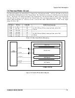
Page 41: ... then 5Vdc Logic voltage is produced 7 1 4 VPRT 8 5VDC 8 5VDC Thermal Printer driving voltage is produced by the step down dc dc converter U4 34063A That is U4 produces rectangular wave at the collector of Q10 A1010 by switching Q6 using 24VDC This makes D3 IN5822 and L6 store energy The voltage is smoothed by C34 470uF and then 8 5VDC thermal printer driving voltage is produced 7 1 5 VPH 8 5Vdc 8...

Page 42: ... sudden power off to backup the needed data and current CPU status into RAM before 35ms just before 5V drops When power is turned on the CPU does the operations which were working before power off This system is designed to sense the time when the AC Line voltage is goes down to 89Vac USA or 170Vac Europe That is when 24Vdc goes down to 14Vdc The waveform of power fail signal refer to Figure 7 2 V...

Page 43: ... Bat t er y Char gi ng W hen PowerO f f VBT Suppl y DI O DE SK14 D28 VCC D13 DI O DE SK14 R104 270 DI O DE SK14 D16 3 6V BAT1 DI O DE SK14 D14 Figure 7 3 Battery Circuit 7 3 2 RTC Clock Circuit This uses an Clock IC RS5C372A is driven by the Battery when the main Power is turned off VCC RTC_SDA RTC_SCLK R96 100 VCC R51 4 7K R92 100 VBT 3 SDA 6 O SCO UT 1 I NTRB 8 VDD 2 SCL 4 VSS 7 O SCI N 5 I NTRA...

Page 44: ...the other Caution Make sure that the Cash Drawer solenoid resistance is more than 20Ω V144 C72 100nF VCC R5 10K VDRV DI O DE M 4 D1 1 CN7 1 VDRV 3 CN7 3 R1 10K R2 4 7K 1 2 3 KSD288 Q 1 DRAW ER SEN_DW RCO M P L4 DRAW ER L1 1 2 3 M M BT2222A Q 5 2 CN7 2 CO N BO X 4P 2 5M M ST YH 4 CN7 4 CO N BO X 4P 2 5M M ST YH Figure 7 6 Cash Drawer Block Circuit 7 3 5 VFD Display Block Circuits This uses 10digit ...

Page 45: ...fic key is pressed during the given time The CPU reads the data through U23 74HC541 and analyzes what key is pressed and transmits this information to the CPU then performs the selected function The Key Board Circuit sends the mode scan signal to the Key lock switch and takes the return data through the U23 74HC541 and performs the selected function Figure 7 8 Keyboard Block Diagram DATA 0 7 74HCT...

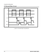
Page 46: ...o the Thermal Printer Then the Printer outputs the Serial Data The Strobe Signals STB1 STB2 STB3 are shorted each other on Main PBA Same STB4 STB5 STB6 Each Strobe Signal manage the Printer Dot STB No DOT No DOTs STB ER 380 Strobe Processing STB1 1 64 64 STB2 65 128 64 STB3 129 192 64 The STB1 STB2 and STB3 are shorted each other on Main PBA 192 Dots STB4 193 256 64 STB5 257 320 64 STB6 321 384 64...

Page 47: ...Circuit Descriptions 7 8 SAM4S ER 380M F SERIES 7 5 Thermal Printer Circuit Figure 7 10 Thermal Printer Timing Waveform CLK DATA LATCH STB1 2 3 STB4 5 6 Printing 1 192 Printing 193 384 384 Bits 384 Bits 384 Bits ...

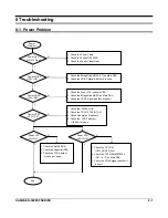
Page 48: ...hether it is short 1 Check the Bridge Diode D4 5 6 7 on Main PBA 2 Check the VDISP signal whether it is short N N Power VPRT 8 5V Ok Power VCC 5V Ok Y Y 1 Check the IC34063 U4 2 Check the TR1010 708 Q10 6 3 Check Generated Frequency 4 Check the VPRT whether it is short or open 1 Check the mc7805 U5 2 Check the Capacitor C50 3 Check the VCC whether it is short or open N Power VPH 8 5V Ok 1 Check th...

Page 49: ... LM393 U17 2 Check the Power 24V 5V 3 Check the related Circuit and Pattern on PWB N N SRAM Ok Y Y N CPU Ok Y N 1 Check the nCS nRD nWR signal of SRAM 2 Check the VBT Battery Volt 3 Check the Decoder IC 74HC138 U11 4 Replace the SRAM Y N 1 Check the Clock 14 7456MHz 2 Check the Power of CPU VCC Pin 5V 3 Check the mounted state of CPU pin whether the pin is open or short RTC Ok 1 Check the nCS nRD ...

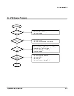
Page 50: ...k the DATA Signal CPU P9 6 3 Check the LATCH Signal CPU P9 7 4 Check the Harness Disconnect Ok Power VDISP VCC Ok Y 1 Refer to the Power Problem 2 Check the Harness 1 Check the Harness 2 Check the VFD Disconnection Signal Pattern N VFD PBA Assy Ok Y 1 Check and Replace the VFD PBA 2 Check the UCL5812 3 Check the VFD 4 Check the Harness Soldering Point N Y N ...

Page 51: ...8 Troubleshooting 8 4 SAM4S ER 380M F SERIES ...

Page 52: ...Check the Harness N Sensor OK 1 Check the related Circuit and Pattern of 74HC14 U9 2 Check the Harness 3 Check the Print Connection PBA and Sensor PBA Y Line Feed OK N 1 Check the Phase Signal CPU P7 4 P7 5 2 Check the Driver LB1838 U6 Enable Signal 3 Check the related Circuit and Pattern IC LB1838 4 Check the Harness 5 Check the Feed Step Motor Y N Thermistor OK 1 Check the ADC Port P10 0 of CPU ...

Page 53: ...turn Part 74HCT541 U23 3 Check the related Circuit and Pattern 4 Check Change Key Board Assy 5 Check the KBD Connector on PBA Specific Key Failure 1 Check the affected Key 2 Check the Matrix Bus Data Bus 3 Check the Diodes D20 D27 4 Check the Key Board Assy N Mode Key Ok Y Y 1 Check the Harness Mode Key Assy 2 Check Diode D12 3 Check the 74HCT541 Data Bus CPU P10 3 N ...

Page 54: ...8 Troubleshooting SAM4S ER 380M F SERIES 8 7 ...

Page 55: ...ck the related circuit Component KSD288 Q1 MMBT222A Q5 on Main PBA 3 Check the Solenoid in the Drawer Compulsory Failure 1 Check the Compulsory Harness Connector 2 Check the Micro switch in the Drawer N Y End End Spool Motor Ok Y 1 Check the Spool Motor Signal CPU P1 4 2 Check the Harness 3 Check the related Circuit and Pattern on Main PBA N Spool Motor Problem ...

Page 56: ... Connector 3 Check the TXD RXD Pin on CPU 4 Check the MAX232 Driving Chip and related Circuit on I F PBA Communication Failure 1 Check the connection of the RS 232C and Other side 2 Check the I F Cable whether it is open or short 3 Check whether Signal is affected by the Cable Noise N H W Handshake Ok Y Y 1 Check the connection of the H W handshaking Line and Other side 2 Check the I F Cable wheth...

Page 57: ...8 Troubleshooting 8 10 SAM4S ER 380M F SERIES MEMO ...

Page 58: ...SAM4S ER 380M F SERIES 9 1 9 Exploded Views and Parts List 9 1 Main Set 9 1 1 1 Exploded View Figure9 1 Total Disassembly ER 380M ...

Page 59: ...9 Exploded Views and Parts List 9 2 SAM4S ER 380M F SERIES 9 1 1 2 Exploded View Figure9 2 Total Disassembly ER 380F ...

Page 60: ...T1 2 1 Y B 2 JK72 40207K PMO COVER MODE S W ER 380M HIPS IVR V0 1 Y ER 380M B 3 6002 000319 SCREW TAPPING PH 2 M3 L8 ZPC YEL 2 Y B 4 JK70 10004A IPR BRKT MODE_S W SBHG 1 T1 1 Y B 5 6002 000319 SCREW TAPPING PH 2 M3 L8 ZPC YEL 2 Y B 6 6002 000172 SCREW TAPPING PH 2S M4 L15 1 Y B 7 JK96 10044A MODE KEY ASSY ER 380 NO CORE YH 1 Y B 8 JK72 40209B PMO WINDOW TURRET PC 1 Y B 9 JK92 00970B PBA SUB TURRET...

Page 61: ...PH 2 M3 L8 ZPC YEL 2 Y B 6 6002 000172 SCREW TAPPING PH 2S M4 L15 1 Y B 7 JK96 00956A ELA ETC MODEKEY ASSY ER 380 1 Y B 8 JK72 40209B PMO WINDOW TURRET PC 1 Y B 9 JK92 01231A PBA SUB TURRET ER 380 1 Y B 10 JK72 00015A PMO TURRET BODY HIPS V0 1 Y B 11 6001 000367 SCREW MACHINE FH M4 L10 1 Y B 12 JK70 40305A ICT SHAFT MOLDING SUM 24L FISCAL 1 Y B 13 JK72 00012B PMO CASE UPPER ER 380 FISCAL 1 Y B 14 ...

Page 62: ...603A HARNESS DRA COMP ER 380 4P 180mm PUR BRN 1 Y E 5 6003 001149 SCREW TAPTITE PWH S M4 L10 ZPC YEL SR 1 Y E 6 JK72 40205A PMO CASE FISICAL BOARD HIPS V0 1 Y JK92 00131A PBA SUB FISICAL B D 512K BYTE 1 Y E 7 JK92 00983A PBA MAIN 1M FISICAL 1M BYTE 1 Y E 8 JK92 01260A PBA MAIN BOARD ER 380M FISCAL 1 Y E 9 6006 000199 SCREW ASS Y TAPT WT BH M4 L8 ZPC YEL 2 Y JK26 00013A TRANS POWER USA 120V 60Hz 1 ...

Page 63: ...0171 SCREW TAPPING PH 2S M4 L10 ZPC YEL 1 Y E 20 JK70 10002A IPR BRKT CASING ER 380 SBHG 1 T1 6 1 Y E 21 JK70 20018A IPR BRKT TRANS ER 380 SECC T1 6 1 Y JK39 10002A CBF POWER CORD AUSTRALIA 1 Y JK39 10003A CBF POWER CORD USA 1 Y JK39 10008A CBF POWER CORD UK 1 Y E 22 JK39 10501A CBF POWER CORD EUROPE 1 Y E 23 JK96 10035A ELA MOTOR ASS Y ER 380 1 Y E 24 JK72 40206A PMO HOLDER MOTOR HIPS V0 1 Y E 25...

Page 64: ...9 Exploded Views and Parts List SAM4S ER 380M F SERIES 9 7 9 2 Printer STM 210 9 2 1 Exploded View Figure9 6 Printer STM 210 ...

Page 65: ...3A PMO CAP LEVER HIPS HB BLUE 1 Y C 5 JK60 00003A SCREW SPECIAL SUM 24L WHITE 2 Y C 6 JK70 20003A IPR BRACKET HOOK SECC T1 0 1 Y C 7 JK70 50011A SCREW TAPPING PH 2 M2 L4 WHITE 2 Y C 8 6001 000665 SCREW MACHINE PWH 2 M3 L4 ZPC YEL 2 Y C 9 JK70 20002A IPR FIXED CUTTER SECC T1 2 1 Y C 10 JK70 50004A POLY WASHER Φ3 1 RED 2 Y C 11 JK70 20001A IPR COVER HOUSING SECC T1 0 1 Y C 12 JK70 70001A ICT SHAFT H...

Page 66: ...ENSOR 1 Y C 30 JK70 50009A SCREW MACHINE RH 2 M2 L4 WHITE 1 Y C 31 JK97 10004A ASS Y TPH STM 210 1 Y C 32 JK39 40554A CBF SIGNAL PRINTER FFC 21P 120MM 1 Y JK97 10004B ASS Y TPH HEAT SINK STM 210 1 Y JK47 10001A TPH ROHM 1 N JK70 50005A TPH TAPE 3M 1 N C 33 JK70 20006A HEAT SINK ZNDC 1 N C 34 JK70 30002A SPRING TPH SWP 2 Y C 35 JK70 20005A IPR BRACKET REAR SECC T1 0 1 Y C 36 6001 000665 SCREW MACHI...

Page 67: ...hermal Printer Head assembly replacement 1 Unscrew the bolt of COVER FRONT and disassemble it from the PRINTER 2 Open the COVER TOP 3 Disassemble the TPH assembly by pulling the lower part of TPH assembly and lift it up 4 Assemble the TPH assembly in reverse order and close the COVER TOP ...

Page 68: ...9 Exploded Views and Parts List SAM4S ER 380M F SERIES 9 11 9 3 Key Board 9 3 1 Key Board 44Key 9 3 1 a Exploded View D 1 D D 2 D 3 D 4 D 8 D 5 D 9 D 10 D 11 D 12 D 6 D 7 Figure9 8 Key Board 60 Key ...

Page 69: ... D 2 LABEL KEY TOP SET ER 380 1 N D 3 JK81 20013A KEY TOP ASS Y S 1X1 30 Y D 4 JK81 10285T SPRING RETURN 1X1 42 Y D 5 JK81 10946A KEY CAP L 1X2 1 Y D 6 JK81 20014A KEY TOP ASS Y L 1X2 1 Y D 7 JK81 20001A SPRING RETURN 1X2 2 Y JK81 10933A KEY TOP 1 1 Y JK81 10934A KEY TOP 2 1 Y JK81 10935A KEY TOP 3 1 Y JK81 10936A KEY TOP 4 1 Y JK81 10937A KEY TOP 5 1 Y JK81 10938A KEY TOP 6 1 Y JK81 10939A KEY TO...

Page 70: ...8 c2 c1 c3 Figure9 13 Drawer 4B 8C b2 b1 b11 b12 b5 b3 b4 b7 b8 b6 b9 c ASS Y HOUSING e ASS Y BOTTOM d ASS Y LOCK b ASS Y TRAY TILL b10 e1 e5 e2 e3 e4 e7 e6 e8 d1 d2 d3 d4 d11 d6 d7 d9 d10 d5 d8 c2 c1 c3 a8 a4 a5 a3 a2 a6 a7 a1 a ASS Y BILL COIN 5B5C Figure9 14 Drawer 5B 5C a1 a4 a5 a ASS Y BILL COIN 7B8C a3 a2 b2 b1 b11 b12 b5 b3 b4 b7 b8 b6 b9 c ASS Y HOUSING e ASS Y BOTTOM d ASS Y LOCK b ASS Y ...

Page 71: ...BILL COIN A TYPE 7B8C 1 Y a 1 6002 000175 SCREW TAPPING PWH 2 M3 L8 ZPC YEL 3 Y a 2 JK70 00068A IPR HOLDER PLATE A TYPE SBHG 1 T1 2 1 Y a 3 JK72 00083A PMO BILL PARTITION A TYPE HIPS BLK 5 Y a 4 JK72 00082A PMO BILL TILL A TYPE HIPS BLK 2 Y a 5 JK72 00084A PMO BILL COIN TILL A TYPE HIPS BLK 1 Y 9 5 2 b ASS Y TRAY TILL No Code No Description Specification Q ty Design Location Serviceable Remark JK9...

Page 72: ...LATCH LONG LEVER 1 N d 4 JK75 00027B MEC LOCK LEVER A TYPE 2 LATCH SHORT LEVER 1 N d 5 6107 001014 SPRING ES Φ0 4 D4 8 L18 1 Y d 6 JK33 10500A SOLENOID DC A DRAWER 1 Y d 7 6001 000131 SCREW MACHINE BH 2 M3 L6 ZPC YEL 2 Y d 8 6001 000525 SCREW MACHINE PH 2 M3 L14 ZPC YEL 2 Y d 9 3405 001013 SWITCH MICRO 125V 5A 1 Y d 10 JK39 40301R CBF HARNESS 2P 150MM BRN 1007 1 Y d 11 6002 000161 SCREW TAPPING PH...

Page 73: ...9 Exploded Views and Parts List 9 16 SAM4S ER 380M F SERIES MEMO ...

Page 74: ...SAM4S ER 380M F SERIES 10 1 10 PCB Layout and Parts List 10 1 Main PCB Layout 10 1 1 MAIN PCB PCB JK41 10552A 10 1 1 a Component Side View ...

Page 75: ... M51953B SIP 5P PLASTIC 18V 1 U8 2001 000027 R CARBON 100OHM 5 1 4W AA TP 2 4X6 4MM 1 R10 2001 001291 R CARBON 1OHM 5 1 2W AA TP 3 5X9 5MM 1 R35 2003 000502 R METAL OXIDE S 150ohm 5 2W AA TP 4x12 1 R26 2005 001001 R WIRE WOUND 0 1ohm 5 1W AA TP 3 3x9mm 1 R20 2005 001001 R WIRE WOUND 0 1ohm 5 1W AA TP 3 3x9mm 1 R21 2005 001001 R WIRE WOUND 0 1ohm 5 1W AA TP 3 3x9mm 1 R22 2301 000010 C FILM PEF 100n...

Page 76: ...5mm STRAIGHT RE 1 CN11 4302 000126 BATTERY NICD 2ND 3 6V 1 2Vx3 60mAH CYL 1 BAT1 JK27 60100D COIL FILTER ER 350 140 UH 1 L5 JK96 10039A ELA HOU HEATSINK ER 380 7805 KSA1010Y 1 U5 7805 1203 000001 IC POSI FIXED REG 7805 TO 220 3P PLAS 1 0502 000234 TR POWER KSA1010Y PNP 40W TO 220 TP 100 1 6002 000175 SCREW TAPPING PWH 2 M3 L8 ZPC YEL 2 0205 000003 OIL SILICON G746 1 6203 000107 HEAT SINK NONE T2 W...

Page 77: ...CHIP 100OHM 5 1 10W DA TP 2012 18 R38 R43 R44 R45 R47 R50 R52 R53 R57 R59 R60 R64 R71 R73 R90 R91 R92 R96 2007 000300 R CHIP 10KOHM 5 1 10W DA TP 2012 33 R1 R3 R5 R6 R9 R11 R13 R25 R27 R29 R30 R33 R36 R40 R46 R56 R58 R63 R65 R66 R69 R70 R75 R77 R79 R81 R84 R89 R94 R95 R105 R125 R130 2007 000355 R CHIP 12KOHM 5 1 10W DA TP 2012 5 R97 R61 R76 R85 R87 2007 000406 R CHIP 15KOHM 1 1 10W DA TP 2012 1 R6...

Page 78: ... C53 C55 C59 C60 C66 C68 C69 C70 C71 C80 2203 000260 C CERAMIC CHIP 10nF 10 50V X7R TP 2012 3 C74 C79 C61 2203 000595 C CERAMIC CHIP 0 22nF 5 50V NP0 TP 2012 1 C54 2203 000634 C CERAMIC CHIP 0 022nF 5 50V NP0 TP 201 1 C51 2203 000634 C CERAMIC CHIP 0 022nF 5 50V NP0 TP 201 1 C52 2203 000938 C CERAMIC CHIP 0 47nF 5 50V NP0 TP 2012 12 C2 C6 C11 C13 C15 C18 C19 C20 C21 C22 C24 C30 2203 000990 C CERAM...

Page 79: ...X 4P 1R 2 5mm STRAIGH 1 CN3 Y 3711 003969 CONNECTOR HEADER BOX 2P 1R 2 5mm STRAIGH 1 CN8 Y 3711 003409 CONNECTOR HEADER BOX 3P 1R 2mm STRAIGHT 1 CN4 Y 3711 004059 CONNECTOR HEADER BOX 30P 2R 2mm ANGLE SN 1 CN2 Y 3711 000965 CONNECTOR HEADER BOX 4P 1R 2 5mm ANGLE 1 CN7 Y 3711 003968 CONNECTOR HEADER BOX 3P 1R 2 5mm STRAIGH 1 CN5 Y 0501 000399 TR SMALL SIGNAL KSC945 G NPN 250mW TO 92 1 Q1 Y 2001 000...

Page 80: ...ts List No Part No Description Specification Q TY Design Location Serviceabl e Remark s JK92 01227B PBA SUB POWER SW ER 5200 5500 STD 1 ASSY Y 3711 000190 CONNECTOR HEADER 1WALL 2P 1R 7 92mm STRA 1 CN3 Y 3711 000829 CONNECTOR HEADER BOX 2P 1R 6 2mm STRAIGH 2 CN1 CN2 Y JK41 10545B PCB POWER SWITCH ER 52 5500 FR 1 1L T1 6 1 Y ...

Page 81: ...1 8P Y JK73 10207A RPR PAD ER 220N SPONGE BLK 2 T5 0 Y 1003 001381 IC VFD HV5812P DIP 28P 540MIL ST PLA 1 U1 Y JK69 90902A PACKING VINYL PET 2126 30X100000XT0 05 1 DIGITRON Y 0402 000208 DIODE RECTIFIER EK 04 40V 1 5A DO 41 1 D2 Y JK94 01120A PHANTOM AU JK92 01240A 1 N 0402 000129 DIODE RECTIFIER 1N4003 200V 1A DO 41 TP 1 D1 Y JC39 40511A CBF HARNESS ML 80 JUMPER AWG22 52mm SILV 5 J1 J2 J3 J4 J5 Y...

Page 82: ...00 5200 FR 1 1L T1 6 1 FUTABA VFD 10 DIGIT Y 10 4 3 ER 380M Rear Display VFD 10Digit 10 4 2 a Component Side View 10 4 2 b Parts List Rear Display No Part No Description Specification Q TY Design Location Serviceable Remarks JK92 00970B PBA SUB TURRET ER 450 WORLD BASIC 1 3711 004109 WAFER BOX HEADER 1R 8P 2 5mm STRAIGHT 1 CN1 WHITE JK07 00005A DISPLAY VFD DC10G FUTABA 10 LT 50GK 1 V1 JK39 40606A ...

Page 83: ...ER 5240F FR 4 2L T1 6mm 348X5 1 Y 10 5 2 b Parts List Memory Size 1MBITs No Part No Description Specification Q TY Design Location Serviceabl e Remark s JK92 00132B PBA SUB FISCAL B D 1MBITs 1 1MBITs ASSY Y 1102 000109 IC EPROM 27C010 128Kx8BIT DIP 32P 600MI 1 U1 Y 0403 000141 DIODE ZENER 1N4735A 6 2V 5 1W DO 41 TP 1 ZD1 Y JK39 40305B CBF HARNESS UL 1007 120 WHT BLU RED 2 1 CN1 Y JK94 00055A PHANT...

Page 84: ...5 1 10W DA TP 2012 1 R4 Y R1 R5 R6 R7 R8 R9 R10 2007 000872 R CHIP 4 7KOHM 5 1 10W DA TP 2012 10 R11 R12 R13 Y 2203 000192 C CERAMIC CHIP 100nF 80 20 50V Y5V TP 1 C2 Y 0404 001051 DIODE SCHOTTKY SK14 40V 1000MA DO 214AA 2 D1 D2 Y 0501 000457 TR SMALL SIGNAL MMBT2222A NPN 350MW SOT 1 Q1 Y JK41 10531B PCB FISCAL ER 5240F FR 4 2L T1 6mm 348X5 1 Y 10 6 Interface Layout 10 6 1 Exploded View 10 6 2 Part...

Page 85: ...10 PCB Layout and Parts List 10 12 SAM4S ER 380M F SERIES MEMO ...

Page 86: ... 24V 30V P fail DETECT SPOOL DRIVE DRAWER BUZZER DRIVE SPOOL MOTOR DRAWER DRIVE BUZZER EPROM M27C4000 SRAM 2MBITS RTC 32 768Khz FISICAL VOLT DRIVE FISICAL I F 82C55 KEY MODE SCAN RETURN BUFFER 74HC541 DECODE 74HC138 FS781 14 7456Mhz FISICAL MEMORY B D 512K 1M 2M SCAN RETURN KEY BOARD MODE KEY D 0 8 DECODE 74HC138 nCS ADD nCS ADD nCS CS_KEYSCAN FA16 17 nCS_EPROM nCS2 SRAM 4MBITS 12 5V 6 2V FA 0 15 ...

Page 87: ... VPRT VDRV VDISP 5V 8 5V 24V 30V P fail DETECT SPOOL DRIVE DRAWER BUZZER DRIVE SPOOL MOTOR DRAWER DRIVE BUZZER EPROM M27C4000 SRAM 2MBITS RTC 32 768Khz FISICAL VOLT DRIVE FISICAL I F 82C55 KEY MODE SCAN RETURN BUFFER 74HC541 DECODE 74HC138 FS781 14 7456Mhz FISICAL MEMORY B D 512K 1M 2M SCAN RETURN KEY BOARD MODE KEY D 0 8 DECODE 74HC138 nCS ADD nCS ADD nCS CS_KEYSCAN FA16 17 nCS_EPROM nCS2 SRAM 4M...

Page 88: ... FA4 10 GND CN3 Drawer 10 FA0 11 PSTROBE 2 No Signal Name 11 CS_FISCAL EPROM 12 PCLK 1 GND 12 FA15 13 GND 2 SEN_DWRCOMP 13 GND 14 GND 3 DRAWER 14 FA14 15 PSTROBE 1 4 VDRV 15 VCC 16 PDATA 16 FA13 17 PLATCH CN5 Black Box 17 VPP 18 GND No Signal Name 18 FA12 19 GND 1 VCC 19 FD3 20 VPH 8 5V 2 TXD1 CLK 20 FA8 21 VPH 8 5V 3 RXD1 DATA 21 FD4 22 VPH 8 5V 4 GND 22 FA9 23 GND 23 FD5 24 MOT_LF_B CN13 14 Keyb...

Page 89: ...12 Wiring Diagram 12 2 SAM4S ER 380M F SERIES MEMO ...

Page 90: ...Block 13 5 4 External In Out Serial I F Block 13 6 5 Key Scan Block 13 7 6 Printer Block 13 8 7 Fiscal I F Block 13 9 8 Power Block 13 10 2 Power Switch PCB Schematics 13 11 3 Display PCB Schematics 1 VFD Front Schematics ER 380F 13 12 2 VFD Rear Schematics ER 380F 13 13 3 VFD Rear Schematics ER 380M 13 14 4 Fiscal PCB Schematics 13 15 5 STM 210 Printer PCB Schematics 13 16 6 Interface PCB Schemat...

Page 91: ...O n O f f Fi scal Ext end Addr ess16 1M Bi t s Al l C l ear Sw i t ch 2 C N 13 B N ot e S0 S1 00 M ean i s i nput cl ock sel ect 6M H z 14M H z C 54 220pF R 49 3 3K R ESET C I R C U I T C 47 100nF C 57 100nF _C S0 _C S3 100uF C 48 16V R EVI SI O N H I STO R Y N ot e AD C VR EF Vol t age i s 5 0V C 65 100nF 100pF C 68 VC C R 44 100 R 50 100 Fi scal Ext end Addr ess17 2M Bi t s 1 C O N N O W ALL 3P ...

Page 92: ... S5C 372A C 73 100nF 32 768KH z X2 A 0 19 LD 0 7 SR AM 3 4M BI Ts SR AM 2 1M BI Ts LC D _EN H I G H C S_SR AM 1 _R ESET A 0 19 V66 V65 7 14 1 3 2 U 12 1 74H C T08 0xC 00000 0xC FFFFF C 62 100nF C 86 100nF 10 9 8 U 12 3 74H C T08 SR AM 1 1M BI Ts D I O D E SK14 D 10 12 13 U 9 6 74H C 14 LD 0 7 R EVI SI O N H I STO R Y R 55 4 7K VBT C 81 100nF C 82 100nF K W on C hoi VBT VC C 22 C E 32 VC C 12 A0 9 ...

Page 93: ... BU ZZER VC C 2003 10 18 K W on C hoi V1 4 VPR T 1K R 39 M M BD 6050LT1 D 9 R 26 150 2W 100uF C 92 16V VPH 4 7K R 37 4 7K R 42 10K R 105 R 86 4 7K 12K R 97 6 8K R 98 VD R V VC C 7 5 6 LM 393D U 17 2 C 85 100nF H I G H Act i ve VPH _O N O FF W hen Pow er O n Bat t er y C har gi ng BU ZZER VPH I c 53 m A M i n hf e 100 5 3 A KSA1010 hf e 100 200 W hen Pow er O f f VBT Suppl y 10K R 40 2 3 1 M M BT22...

Page 94: ...W ER VSER I AL_O FF I N T0_PFAI L 2 C N 5 2 20C N 10 T 14C N 10 N 8C N 10 H 2C N 10 B _R D 245_O E 7 Bl anki ng St r obe 8 D i sconnect SEN _D I SPD I SC O N R 57 100 4 G N D 5 Lat ch D I SPLAY_LATC H 1 Ser i al D at a I n D I SPLAY_D ATA L1 2 3 1 KSA1182 Y Q 2 R 6 10K 1K R 7 1K R 8 D 8 D I O D E M 4 1 C N 5 1 C O N BO X 2P 2 5M M ST YH R EVI SI O N H I STO R Y BackLi t Vol t age 4 2V 240m A 10C N...

Page 95: ... G 5 CN3 E 4 CN3 D 5 CN9 5 4 CN9 4 2 CN9 2 1uF C33 VCC VCC VCC C13 470pF C18 470pF C22 470pF VSERIAL 1 2 3 MMBT2222A Q12 R31 4 7K VSERIAL 1 3 2 KSA708Y Q14 C38 1uF C28 1uF C14 1uF 19 CN8 S 17 CN8 Q 11 CN8 K 13 CN8 M 5 CN8 E 7 CN8 G 7 CN4 G 5 CN4 E RXD1 DSR1 2 CN4 B 4 CN4 D 9 CN4 I 7 CN2 G 5 CN2 E RXD0 DSR0 4 CN2 D 2 CN2 B VSERIAL 9 CN2 I UART 2 C24 470pF C36 1uF C35 1uF C37 1uF C11 470pF C26 1uF C...

Page 96: ...140 V131 M O D E_SI G D 12 2003 10 18 Key R et ur n 4 C N 14 D 7 C N 12 7 4 C N 12 4 K W on C hoi V1 3 D 25 D 26 VC C 4 7K R 122 4 7K R 128 4 7K R 126 4 7K R 107 M ode Key A 0 19 1 C N 13 A C O N FPC 8P 2 54M M ST _C S1 D 6 D 7 D 3 D 4 D 0 D 1 L18 L21 Key Scan 39 R 119 39 R 108 39 R 109 39 R 110 39 R 111 39 R 118 _R D C 93 100nF D 5 D 2 R EVI SI O N H I STO R Y L20 L19 L16 L15 L17 1 C N 14 A C O N...

Page 97: ... K W on C hoi V1 4 C 76 100nF R 56 10K VC C VC C C 80 100pF R 79 10K VC C R 78 470 56K R 82 VPH VC C R 85 150K N ot e EN A1 2 H Act i ve N O TE U 17 2 G ATE i s l ocat ed i n Page 1 SEN _LEVER _I N TPH _PLATC H M O T_B M O T_B M O T_A TPH _PSTB 1 TPH _PSTB 2 M O T_A TPH _TH ER M I STER M O T_A M O T_A M O T_B M O T_B 25 19 TPH _PD ATA TPH _PC LK 13 PEN D _I N _L D I SC O N _I N 7 SEN _LEVER _I N P...

Page 98: ...0 18 FD 0 7 K W on C hoi V1 4 R 129 4 7K VC C C 91 100nF R 108 4 7K 6 8K R 107 VC C 4 7K R 102 V148 V140 _C S2 R ESET FD 0 7 _W R _R D A 1 A 0 D 2 D 1 D 0 D 5 D 4 D 3 D 7 D 6 FA 0 17 Fi scal EPR O M VC C 6 2V 5 3 11 9 15 17 23 21 29 27 1K R 117 VD R V 0x200000 0X2FFFFF hf e 120 240 C 94 100nF D I O D E SK14 D 15 ZD 1 1N 4735A C S_FI SC AL_EPR O M Fi scal EPR O M nC S Fr om C PU Fi scal EPR O M W r...

Page 99: ...P R 19 27K C 34 470uF 16V V1 4 C 4 2200uF 50V VD R V 470uF C 7 50V R 20 0 1 R 22 0 1 VD R V VO U T 1 25 1 R 2 R 1 1 25 1 27K 4 7K 8 43 V VD R V 250V 3 15A FU 1 H S2 H EATSI N K_S 1 I N 3 O U T 2 G N D M C 7805 U 5 C 3 100nF 1 3 2 KSA708Y Q 6 R 15 3 3K H S1 H EATSI N K_S C 27 100uF 50V D 4 M 4 D 7 M 4 100 R 10 C 5 4700uF 50V R EVI SI O N H I STO R Y VPR T R 21 0 1 Pow er Tr anf or m er O ut put 1 2...

Page 100: ... 2 1 1 R ED BLU E BLU E 1 1 2 2 R ED EAR TH BR O W N BLU E 1 3 4 2002 10 16 1 V1 1 PO W ER C O R D AC 230V 50H z 2 2 TO M AI N PBA ER 5500_PO W ER SW SC H K W C H O I ER 5200 PO W ER SW I TC H PC B PO W ER O N O FF SW I TC H 2 1 C N 3 A C O N W ALL 2P 7 92M M 1W ST 2 1 C O N BO X 2P 6 2M M ST C N 1 A 1 C O N BO X 2P 6 2M M ST C N 2 A PO W ER SW I TC H PC B ...

Page 101: ... I f m A P2_B P8_D P P5_C VD I S Vbc 28 4V I bc 24m A O LD PC B I N FO R JK41 10005A V2 2 2001 03 21 AR R AY 4 VFD _STO R BE VFD _LATC H VFD _SC LK VFD _SD I N ER 350 D I SPLAY 10G N ot e The connect i on of R ear D i spl ay PC B i s sam e as O l d Ver si on ER 350 5100 5200 6600 P4_G 1 C N 1 A C O N BO X 8P 2 5M M ST D 2 EK 04 1 C N 3 A C O N BO X 2P 2 5M M ST J19 D i gi t 10 ER 350 380 YES R U S...

Page 102: ...3 G1 G2 G3 VF1 4 CN1 D 7 CN1 G 10 CN1 J 3 CN2 C 6 CN2 F 9 CN2 I P8 com f P1 ER5200REARVFD SCH 1 P5 VCC VCC 2002 10 28 V1 0 2 CN1 B 3 CN1 C 5 CN1 E 6 CN1 F 8 CN1 H 9 CN1 I 11 CN1 K 2 CN2 B 5 CN2 E 4 CN2 D 8 CN2 H 7 CN2 G 10 CN2 J 11 CN2 K VFD REAR PART Hyun Oh Yun 1 CN1 A CON BOX 11P 2MM ST 1 CN2 A CON BOX 11P 2MM ST ER 350 5100 5200 6500 DISPLAY 2 F1 5 P3 4 P2 8 P6 7 P5 11 P9 10 P8 13 G10 16 G7 15...

Page 103: ... P2_B P8_D P P5_C 8 C N 1 H 5 C N 1 E 6 C N 1 F 2 C N 1 B 3 C N 1 C VFD _STO R BE VFD _LATC H VFD _SC LK VFD _SD I N ER 650 5500 D I SPLAY 7 C N 1 G 4 C N 1 D 1 C N 1 A C O N BO X 8P 2 5M M ST 100nF C 2 VC C VFD R EAR PAR T D 2 EK 04 H yun O h Yun VD I SP 2 F1 5 P3 4 P2 8 P6 7 P5 11 P9 10 P8 13 G 10 16 G 7 15 G 8 19 G 4 18 G 5 22 G 1 21 G 2 24 F2 23 F2 1 F1 3 P1 6 P4 9 P7 12 P10 14 G 9 17 G 6 20 G...

Page 104: ... 4 D 1 D I O D E SK14 VC C A16 A13 A7 A4 A1 A10 VC C JP2 0 2002 12 28 D 1 D 4 D 7 V1 1 KSH C KW VC C JP1 0 4 7K R 5 R 10 R 9 0 R 3 A 0 16 D 0 7 C E 4 7K R 1 VC C 100nF AXI AL C 1 512K 1M 2M FI SC AL PC B VC C R 2 560 2 3 1 Q 1 M M BT2222A D 2 D I O D E SK14 R 13 4 7K 8 R 7 R 12 R 6 29 25 23 19 17 13 11 7 5 1 30 24 26 18 20 12 14 6 8 2 27 21 15 9 3 16 22 28 4 10 C N 1 BO AR D I N H AR 30P 31 PG M1 ...

Page 105: ...13 16 SAM4S ER 380M F SERIES ...

Page 106: ...O U T D SR 0_I N VSER I AL VSER I AL 7 C N 4 G 5 C N 4 E 2 C N 4 B 7 C N 3 G 5 C N 3 E 2 C N 3 B 2004 02 23 1 V1 1 R XD 1_I N VSER I AL 4 22 10 16 TXD 0_O U T D SR 0_I N R XD 1_I N VSER I AL 2 3 5 VSER I AL 8 C N 4 H 6 C N 4 F 4 C N 4 D 3 C N 4 C 9 C N 4 I 8 C N 3 H 1 C N 3 A 6 C N 3 F 4 C N 3 D 3 C N 3 C 19 17 11 13 5 7 D SR 1_I N R XD 1_I N TXD 1_O U T D SR 0_I N R XD 0_I N TXD 0_O U T S M K SER...

Page 107: ...13 18 SAM4S ER 380M F SERIES MEMO ...

Page 108: ...s page to record any special servicing information such as Service Bulletins or Supplements When possible record changes to Code numbers directly on the actual Parts List Always record Service Bulletin numbers and Application Dates on this log to ensure that your data is always as current as possible ...

Page 109: ......

Page 110: ...ⓒ Shin Heung Precision March 2004 Printed in KOREA V1 0 Code No JK68 60955A ...

Reviews: