background image

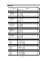
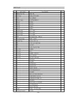
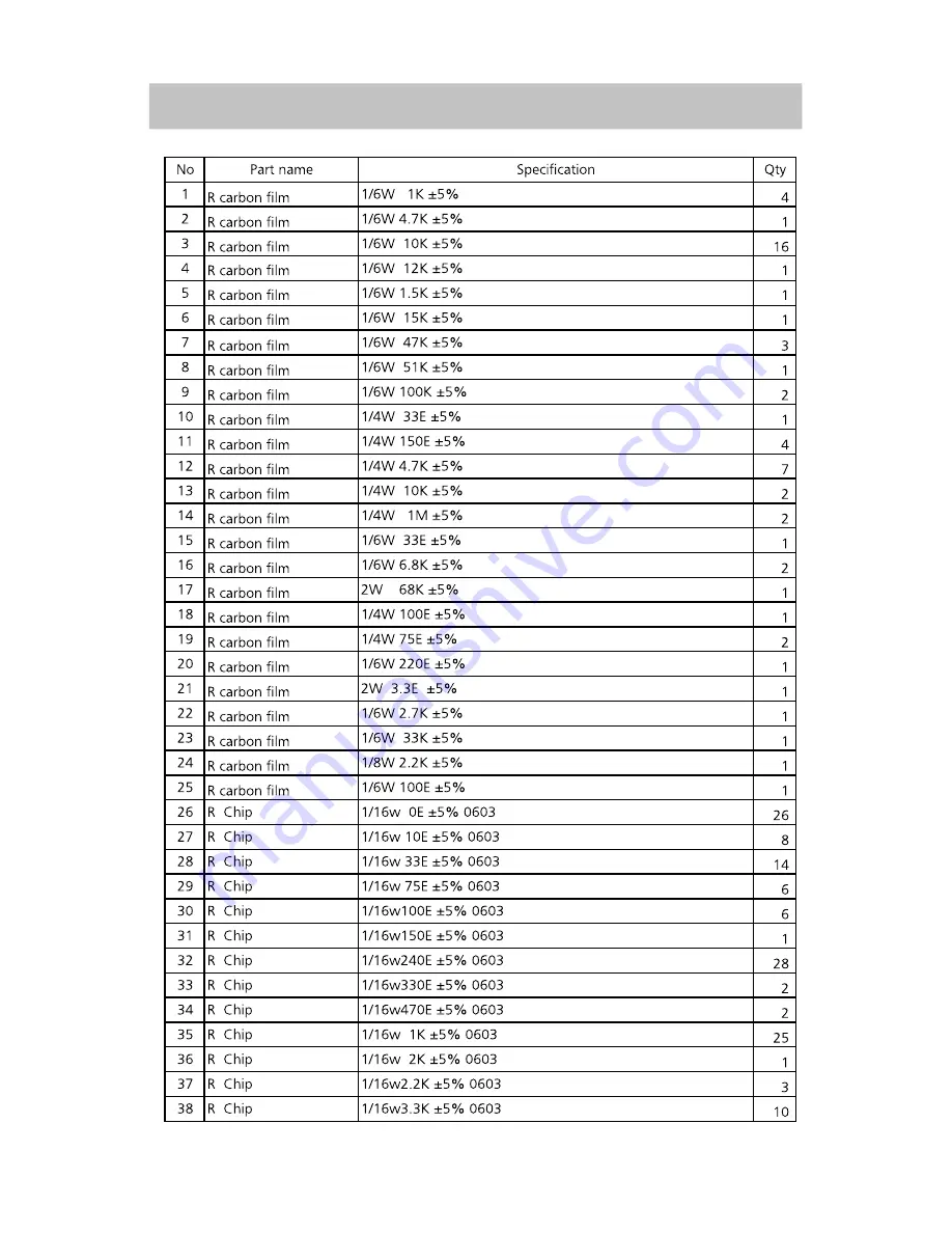
PARTSLIST 

37

Unit:pcs

Summary of Contents for RDV-750

Page 1: ...Service Manual MODEL RDV 750 STAND BY ON VOLUME MIN MAX DVD CD MP3 PLAYER RDV 750 MIC OPEN CLOSE PLAY PAUSE STOP PREV NEXT RUSSIAN OSD LANGUAGE ...

Page 2: ...S 2 ADVANTAGES OF THIS PRODUCT 3 CIRCUIT OPERATIONAL DESCRIPTION 4 VOLTAGE CHARTS 17 CIRCUIT DIAGRAM 18 PCB CIRCUIT BOARD 28 INSTRUMENT DISASSEMBLY 33 PARTSLIST 37 Caution In this Manual some parts can be changed for improving ...

Page 3: ...io out digital audio Video out S video out Microphone1 2 Output Power supply Power consumption Dimensions Gross Weight Net Weight Q JWC RDV 750 Wave length 650nm PAL AUTO NTSC 20Hz 20KHz 1dB 95dB 60 dB 1KHz 85dB 1KHz 80dB 1KHz Output level 2V Load impedance 10KΩ Output level 0 5Vp p Load impedance 75Ω Output level 1Vp p Load impedance 75Ω imbalance negative polarity Output level 1Vp p Chromaticity...

Page 4: ...layback title and chapter for DVD track and disc for VCD CD Repeat a defined period from A to B DVD Selective Play DVD VCD CD You can select and play the desired title chapter of DVD and track of Video CD Various languages OSD On Screen Display function DVD You can select and display OSD among various languages English French Spanish Parental Lock function DVD This function can prevent playback of...

Page 5: ...d to each IC and the SET will be the STANDBY status which requires the least power for input the front panel key input the STAND BY ON key extinguished the LED Once the Power On key is entered u Com recognizes it and initiates each chipset performs sequential algorithms such as determining whether the disc is in or not and if in what type of disc is loaded Through this process it can read disc dat...

Page 6: ...rt term Mecha and Servo Mecha mounts with the optical pick up which allows reading the signal of a disc using laser beam and makes it operates and consists of the deck mechanism which allows loading a disc and reading the data Servo is a sort of circuit which allows operating the loader and recovering the data and consists of Motor Drive IC operating the spindle the sled the loading motor 5 ...

Page 7: ...or opening and closing of the tray The focus signal the tracking signal the sled signal and the spindle signal are input into each relaxant port of the drive IC in the order of No 26 pin 23 4 and 1 and set the gain amplification and the center voltage through the internal OP AMP and drive on both sides and then the focus signal and the tracking signal will be output as VOFC VOFC and VOTK VOTK on a...

Page 8: ...d housekeeping functions The Vibratto II DVD processor is built on the ESS proprietary dual CPU Programmable Multimedia Processor PMP core consisting of 32 bit RISC and 64 bit DSP processors and offers the best DVD feature set The processing units enable simultaneous parallel execution of system commands and data processing to perform specialized enconding and decoding tasks The RISC processor per...

Page 9: ...8 CIRCUIT OPERATIONAL DESCRIPTION ES6629 Vibratto II system Block Diagram ES6629 Vibratto II Block Diagram ES6629 ...

Page 10: ...ror detection for DVD The ES6603 also provides an AC coupled differential or single ended RF signal input to the programmable attenuator with external AC coupling circuitry and an AC coupled single ended input for RF signals The attenuator outputs are AC coupled to the AGC inputs The AC coupled DVD and CD inputs are multiplexed in the input stage for accurate error detection The programmable bandw...

Page 11: ...CIRCUIT OPERATIONAL DESCRIPTION DVD Servo AFE IC ES6603 Block Diagram 10 ...

Page 12: ...CIRCUIT OPERATIONAL DESCRIPTION 11 ES6603 ES6629 Block Diagram ...

Page 13: ...of 16 bits each The A29800UV 70 offers the RESET function The 1024 Kbytes of data are further divided into nineteen sectors for flexible sector erase capability The 8 bits of data appear on I O0 I O7 while the addresses are input on A1 to A18 the 16 bits of data appear on I O0 I O15 The A29800UV 70 is offered in 44 pin SOP and 48 Pin TSOP packages This device is designed to be programmed in system...

Page 14: ...scription The S524C20D21serial EEPROM has a 2 048 bit 256 byte capacity supporting the standard I C bus serial interface It is fabricated using Samsung most advanced CMOS technology One of its major feature is a hardware based write protection circuit for the entire memory area Hardware based write protection is controlled by the state of the write protect WP pin Using one page write mode you can ...

Page 15: ...T H is organized as 4banks of 1 048 576x16 HY57V641620HGT H is offering fully synchronous operation referenced to a positive edge of the clock All inputs and outputs are synchro nized with the rising edge of the clock input The data paths are internally pipelined to achieve very high bandwidth All input and output voltage levels are compatible with LVTTL Programmable options include the length of ...

Page 16: ...HY57V641620HGT H Block Diagram CIRCUIT OPERATIONAL DESCRIPTION 15 ...

Page 17: ... to work with MPEG2 AC 3 decoded data in applications such as DVD player home theater set top box and digital TV etc DA1196 integrates 6 DA channels providing customers a solution of both simplicity and excellent performance DA1196 Block Diagram CIRCUIT OPERATIONAL DESCRIPTION ...

Page 18: ...umber Output voltage 1 2 3 4 5 6 7 8 9 GND S5V 3 3V D5V GND A5V GND 12V 12V J2 Pin number Output voltage 1 2 3 4 5 6 SW F F GND 24V STB5V Decode board input voltage CN1 Pin number Output voltage 1 2 3 4 5 6 7 8 9 GND S5V 3 3V D5V GND A5V GND 12V 12V 17 ...

Page 19: ...1 POWER SUPPLY SCHEMATIC DIAGRAM CIRCUIT DIAGRAM 18 ...

Page 20: ...2 DECODE BOARD SCHEMATIC DIAGRAM CIRCUIT DIAGRAM 1 Vibratto II 19 ...

Page 21: ...2 ES6603 and motor drivers CIRCUIT DIAGRAM 20 ...

Page 22: ...3 Audio and Power CIRCUIT DIAGRAM 21 ...

Page 23: ...4 Audio filter and output CIRCUIT DIAGRAM 22 ...

Page 24: ...5 Flash SDRAM CIRCUIT DIAGRAM 23 ...

Page 25: ...6 SCART CIRCUIT DIAGRAM 24 ...

Page 26: ...3 CONTROL BOARD SCHEMATIC DIAGRAM CIRCUIT DIAGRAM 25 ...

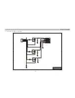
Page 27: ...4 MICROPHONE BOARD SCHEMATIC DIAGRAM CIRCUIT DIAGRAM 26 ...

Page 28: ...5 YUV BOARD SCHEMATIC DIAGRAM CIRCUIT DIAGRAM 27 ...

Page 29: ...1 POWER SUPPLY BOARD PCB CIRCUIT BOARD 28 ...

Page 30: ...2 DECODE BOARD PCB CIRCUIT BOARD 29 ...

Page 31: ...3 CONTROL BOARD PCB CIRCUIT BOARD 30 ...

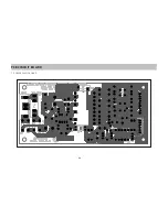
Page 32: ...4 MICROPHONE BOARD PCB CIRCUIT BOARD 31 ...

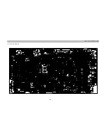
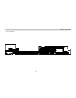
Page 33: ...5 YUV VIDEO OUTPUT BOARD PCB CIRCUIT BOARD 32 ...

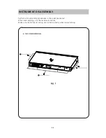
Page 34: ...INSTRUMENT DISASSEMBLY 33 Perform all disassembly procedures in the order presented When reassembling use the reverse procedure Make sure that all leads wiring are routed correctly when reassembling ...

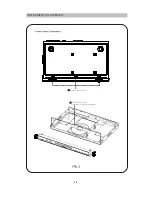
Page 35: ...INSTRUMENT DISASSEMBLY 34 Remove three hooks Remove two hooks Simultaneously remove panel ...

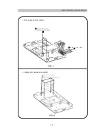
Page 36: ...INSTRUMENT DISASSEMBLY 35 C DECODE BOARD DISASSEMBLY D POWER SUPPLY BOARD DISASSEMBLY Remove five screws Remove four screws Remove power supply board ...

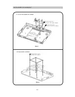
Page 37: ...ENT DISASSEMBLY 36 E YUV OUTPUT BOARD DISASSEMBLY F DVD LOADER DISASSEMBLY FIG 5 FIG 6 Remove two screws Remove SCART output board Remove four screws Remove DVD loader Remove one screw Remove YUV output board ...

Page 38: ...PARTSLIST 37 Unit pcs ...

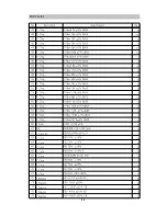
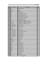
Page 39: ...38 PARTSLIST ...

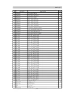
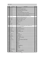
Page 40: ...39 PARTSLIST ...

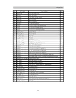
Page 41: ...40 PARTSLIST ...

Page 42: ...41 PARTSLIST ...

Page 43: ...42 PARTSLIST ...

Page 44: ...43 PARTSLIST ...

Reviews: