background image

A-70

Sept, 1997

SERVICE NOTES

TABLE OF CONTENTS

Page

SPECIFICATIONS

1

DISASSEMBLY

1

LOCATION OF CONTROLS & REAR VIEW

2

EXPLODED VIEW N.1

3

EXPLODED VIEW N.2

4

KEYBOARD PARTS LIST

4

BLOCK DIAGRAM

5

MAIN PCB ASSY 

6

CIRCUIT DIAGRAM (MAIN PCB ASSY)

7

PRIMARY PCB ASSY & CIRCUIT DIAGRAM

8

LEFT CONTROL PCB ASSY

8

CIRCUIT DIAGRAM (LEFT CONTROL PCB ASSY)

9

AFT PCB ASSY & CIRCUIT DIAGRAM

10

RIGHT CONTROL PCB ASSY

10

CIRCUIT DIAGRAM (RIGHT CONTROL PCB ASSY)

11

POWER PCB ASSY & CIRCUIT DIAGRAM

12

MIDI PCB ASSY

12

CIRCUIT DIAGRAM (MIDI PCB ASSY)

13

RIGHT CONTACT PCB ASSY w/RUBBER CONTACT & CIRCUIT DIAGRAM

14

LEFT CONTACT PCB ASSY w/RUBBER CONTACT & CIRCUIT DIAGRAM

14

TEST MODE

15/20

PARTS LIST

20/21

TRANSLATION FROM ENGLISH INTO JAPANESE

22/27

S P E C I F I C AT I O N S

A - 7 0 / A - 7 0 E X   :   E x p a n d a b l e   c o n t r o l l e r

A - 7 0 E X   S o u n d   S e c t i o n   ( V E - R D 1 )

- S o u n d   G e n e r a t o r

P C M   s y n t h e s i s

- P a r t s

4   P a r t s

- M a x i m u m   P o l y p h o n y

6 4   Vo i c e s .

- E f f e c t s

R e v e r b
C h o r u s
E q u a l i z e r

- P r e s e t   M e m o r y

P a t c h e s

:   1 2 8

A - 7 0 / A - 7 0 E X   C o m m o n

- K e y b o a r d

7 6   K e y s

- Z o n e s

I n t e r n a l

:   4

E x t e r n a l

:   4

- I n t e r n a l   M e m o r y

S y s t e m   S e t u p

:   1

U s e r   N a m e   M a p s

:   4

P r e s e t   N a m e   M a p s

:   9

P e r f o r m a n c e s

:   6 4

C h a i n s

:   1 0

M a n u a l

:   1

- D i s p l a y

3   C h a r a c t e r s   ( b a c k l i t   L C D )
1 7   C h a r a c t e r s ,   2   L i n e s   ( b a c k l i t   L C D )

.

- N o m i n a l   O u t p u t   L e v e l

O u t p u t

:   - 7 d B m .

- O u t p u t   I m p e d a n c e

O u t p u t

:   1 6 0 0   O h m .

- R e c o m m e n d e d   L o a d   I m p e d a n c e

O u t p u t

:   1 0   K o h m   o r   G r e a t e r

- C o n n e c t o r s

M i d i   C o n n e c t o r s   ( i n : 2 ,   t h r u : 1 ,   o u t : 4 )
F o o t   C o n t r o l l e r   J a c k s : 1
S w i t c h   J a c k s : 1
To t a l   Vo l u m e   P e d a l   J a c k
H o l d   P e d a l   J a c k
O u t p u t   J a c k s   [ L ( M o n o ) ,   R ]
H e a d p h o n e   J a c k
A C   I n l e t   ( A C   1 0 0 V,   A C   2 3 0 V,   A C   2 4 0 V )

- P o w e r   S u p p l y

A C   1 0 0 V,   A C   11 7 V,   A C   2 3 0 V   o r   A C 2 4 0 V

- P o w e r   C o n s u m p t i o n

1 5 W   ( A C   1 0 0 V ) ,   1 7 W   ( A C   11 7 V )
2 0 W   ( A C   2 3 0 V ) ,   2 0 W   ( A C   2 4 0 V )

- D i m e n s i o n s

1 2 4 5 ( W )   X   3 5 7   ( D )   X   1 3 6   ( H )   m m

- We i g h t

1 6   K g

- A c c e s s o r i e s

P e d a l   S w i t c h : D P - 2

( 7 7 1 0 6 1 0 0 0 0 )

O w n e r ’s   M a n u a l   ( E )

( K 6 0 1 8 2 8 8 )

O w n e r ’s   M a n u a l   ( J )

( K 6 0 1 8 2 9 1 )

M i d i   G u i d e

( K 6 0 1 8 1 0 9 )

M i d i   I m p l e m e n t a t i o n   M a n u a l

( K 6 0 1 8 2 9 2 )

!

MAINS CABLE H05VV+POL.SOCKET

230V

(J3439150)

!

CABLE 49B/35JT 2X18 AWG-C17

117V

(J3439128)

!

MAINS CABLE DC 545 J03

100V

(13499108)

!

CABLE BS/13/H05VV-F3G 0.75-V

230VE

(13499152RI)

!

CABLE SAA/3-OA3CCFC 3X0.75-V

240VA

(13499150RI)

- O p t i o n s

S t e r e o   H e a d p h o n e

:   R H - 2 0 / 8 0 / 1 2 0 :

P e d a l   S w i t c h

:   D P - 2 / 6 ,   B O S S   F S   5 U

E x p r e s s i o n   p e d a l

:   E V - 5

C o n n e c t i n g   C a b l e

:   P J - 1 M ,   P C S - 1 0 0 P W

M I D I / S Y N C   c a b l e

:   M S C - 1 5 / 2 5 / 5 0

Vo i c e   E x p a n s i o n   b o a r d

:   V E   s e r i e s

Issued by RES

Copyright © 1997 by ROLAND CORPORATION

DISASSEMBLY

1

SN00018

K6018299

Printed in Italy (AF00) (AD)

First Edition

Summary of Contents for A-70

Page 1: ...aps 9 Performances 64 Chains 10 Manual 1 Display 3 Characters backlit LCD 17 Characters 2 Lines backlit LCD Nominal Output Level Output 7dBm Output Impedance Output 1600 Ohm Recommended Load Impedance Output 10 Kohm or Greater Connectors Midi Connectors in 2 thru 1 out 4 Foot Controller Jacks 1 Switch Jacks 1 Total Volume Pedal Jack Hold Pedal Jack Output Jacks L Mono R Headphone Jack AC Inlet AC ...

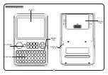
Page 2: ...2 A 70 Sept 1997 LOCATION OF CONTROLS REAR VIEW ...

Page 3: ...3 A 70 Sept 1997 EXPLODED VIEW N 1 ...

Page 4: ...4 A 70 Sept 1997 KEYBOARD PARTS LIST 76 KEY KEYBOARD TP 8S AT 7699510000 EXPLODED VIEW N 2 ...

Page 5: ...5 A 70 Sept 1997 BLOCK DIAGRAM ...

Page 6: ...ting benyttes kun batteri som anbefalt av apparatfabrikanten Brukt batteri returneres apparatleverandøren VARNING Eksplosionsfara vid felaktigt batteribyte Använd samma batterityp eller en ekvivalent typ som rekommenderas av apparattillverkaren Kassera använt batteri enligt fabrikantens instruktion VAROITUS Paristo voi räjähtää jos se on virheellisesti asennettu Vaihda paristo ainoastaan laitevalm...

Page 7: ...A B C D E F G H I L M N O P Q R S T U J K 1 2 3 4 5 6 7 8 9 10 12 13 14 15 16 17 18 19 20 21 22 23 24 25 26 27 28 29 30 7 11 A 70 Sept 1997 MAIN PCB ASSY CIRCUIT DIAGRAM ...

Page 8: ... 6 7 8 9 10 12 13 14 15 16 17 18 19 20 21 22 23 24 25 26 27 28 29 30 8 11 A 70 Sept 1997 LEFT PCB ASSY ASSY 7699504000 PRIMARY PCB ASSY CIRCUIT DIAGRAM ASSY 7699506000 230V 240V ASSY 7699512000 100V 117V View from component side View from component side ...

Page 9: ...A B C D E F G H I L M N O P Q R S T U J K 1 2 3 4 5 6 7 8 9 10 12 13 14 15 16 17 18 19 20 21 22 23 24 25 26 27 28 29 30 9 11 A 70 Sept 1997 CIRCUIT DIAGRAM LEFT PCB ASSY ...

Page 10: ...S T U J K 1 2 3 4 5 6 7 8 9 10 12 13 14 15 16 17 18 19 20 21 22 23 24 25 26 27 28 29 30 10 11 A 70 Sept 1997 AFT PCB ASSY CIRCUIT DIAGRAM ASSY 7699507000 RIGHT PCB ASSY ASSY 7699503000 View from component side View from component side ...

Page 11: ...A B C D E F G H I L M N O P Q R S T U J K 1 2 3 4 5 6 7 8 9 10 12 13 14 15 16 17 18 19 20 21 22 23 24 25 26 27 28 29 30 11 11 A 70 Sept 1997 CIRCUIT DIAGRAM RIGHT PCB ASSY ...

Page 12: ... T U J K 1 2 3 4 5 6 7 8 9 10 12 13 14 15 16 17 18 19 20 21 22 23 24 25 26 27 28 29 30 11 A 70 Sept 1997 POWER PCB ASSY CIRCUIT DIAGRAM ASSY 7699502000 JACK PCB ASSY ASSY 7699505000 12 View from component side View from component side ...

Page 13: ...A B C D E F G H I L M N O P Q R S T U J K 1 2 3 4 5 6 7 8 9 10 12 13 14 15 16 17 18 19 20 21 22 23 24 25 26 27 28 29 30 13 11 A 70 Sept 1997 CIRCUIT DIAGRAM JACK PCB ASSY ...

Page 14: ... 17 18 19 20 21 22 23 24 25 26 27 28 29 30 14 11 A 70 Sept 1997 LEFT CONTACT PCB ASSY w RUBBER ASSY 7695005000 CIRCUIT DIAGRAM LEFT CONT PCB ASSY CIRCUIT DIAGRAM RIGHT CONT PCB ASSY RIGHT CONTACT PCB ASSY w RUBBER ASSY 7695004000 View from component side View from component side ...

Page 15: ...y Summary Display the version and test items in the LCD Procedure Press numeric key 0 to display the menu ê The system program version and the test item menu will be displayed ê The test program will wait for an item to be selected 1 SW LED test Summary Check LED and switch operation Procedure Press numeric key 1 to enter the SW LED test item ê All LEDs will light Check that there are no LEDs that...

Page 16: ...O to set the MAX value 16 A 70 Sept 1997 ê This completes the bender settings TRANSPOSE MONO PORTAMENTO NOTE After setting the bender values be sure to perform the bender wheel test to check operation If after performing the bender wheel test you were unsuccessful in making the setting use the following procedure to manually set the dead region Manual adjustment of the dead region 1 Use the cursor...

Page 17: ... appropriate for each key is output If there is a problem refer to check 1 ê Apply pressure to a desired key and check that aftertouch changes in the range 0 to over 6 See NOTE1 If there is a problem refer to check 2 ê This ends the keyboard test If a VE series unit is installed in the A 70 and the OUTPUT jack is connected to an amp a piano sound will be heard Action check 1 KEYBOARD MAIN BOARD CN...

Page 18: ...L L VR701 SAVING AND LOADING USER DATA You can send the contents of internal memory to a sequencer or MIDI device that can record bulk data Data that has been recorded in this way can be received via MIDI IN2 at any time The contents of the internal memory are overwritten by any data that is received This procedure will save the following data to sequencer Performance and Chain setting in the temp...

Page 19: ..._00002 mid _00008 mid _00008 mid will always exist and _00001 _00007 mid may or may not exist depending on the program size Update procedure 0 As necessary save the user memory to a sequencer The contents of user memory will be lost during the software update 1 Connect pedals or mono dummy open plugs to the HOLD and FS jacks of the A 70 2 Connect the MIDI OUT of the SMF player to the MIDI IN2 of t...

Page 20: ...70 7699507000 BOUNCE TO AFTERTOUCH ASSY A 70 7695004000 RIGHT CONTACT BOARD W RUBBER ASSY 7695005000 LEFT CONTACT BOARD W RUBBER ASSY 7699501000 MAIN BOARD PCB ASSY A 70 NOTE When you replace the MAIN BOARD or Lithium Battery You must reperform bender adjustment Refer to Bender Value Setting item in the Test Mode IC 15229718RI I C 6N 137 Photo Coupler IC101 102 on JB 00342723 I C MB90705 H Cpu FMC...

Page 21: ...MA 406 X1 on MB FUSE FUSE HOLDER 12559606RI FUSE 5X20 315MAL 250V SEMKO For 230 240V F1 on P B 12559607RI FUSE 5X20 600MA 250V ULCSA For 100 117V F1 on P B 12199597RI FUSE HOLDER T P1 on P B CONNECTOR 13419677RI 16P FEM CONN AMP P 1 27 CN3 11 on MB CN705 on LB CN1 on LCB 13369689RI 20P FEM CONN AMP P 1 27 CN2 5 8 on MB CN707 on LB CN201 on RB CN2 on RCB J3439108 14P MALE CONN P 1 27 CN6 on MB J343...

Page 22: ...22 A 70 Sept 1997 ...

Page 23: ...A 70 Sept 1997 23 ...

Page 24: ...24 A 70 Sept 1997 ...

Page 25: ...A 70 Sept 1997 25 ...

Page 26: ...26 A 70 Sept 1997 ...

Page 27: ...A 70 Sept 1997 27 ...

Reviews: