


RF-BM-S02
Shenzhen RF-star Technology Co., Ltd.
Page 5 of 23
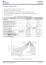
4.7 Soldering and Reflow Condition
Table of Figures
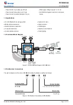
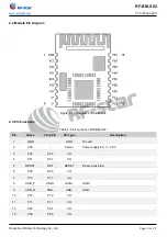
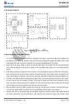
Figure 1. Functional Block Diagram of RF-BM-S02
..................................................................................... 3
Figure 2. Part Number Conventions of RF-BM-S02
.................................................................................... 3
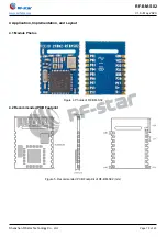
Figure 3. Pin Diagram of RF-BM-S02
Figure 5. Recommended PCB Footprint of RF-BM-S02 (mm)
.............................................................. 13
Figure 6. Schematic Diagram of RF-BM-S02
............................................................................................... 14
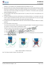
Figure 7. Recommendation of Antenna Layout
........................................................................................... 15
Figure 8. Recommended Reflow for Lead Free Solder
............................................................................ 17
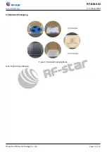
Figure 9. Optional Packaging Mode


