


nRF52810
Shenzhen RF-star Technology Co., Ltd.
Page 13 of 50
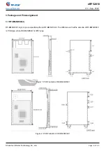
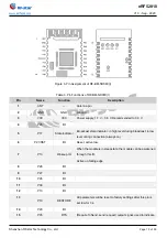
Figure 6. Pin Assignment of RF-BM-ND08C(I)
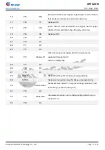
Table 3. Pin Functions of RF-BM-ND08C(I)
Pin
Name
Function
Description
1
ANT
—
Antenna pin
2
GND
GND
Ground
3
VCC
VCC
Power supply: 1.7 V ~ 3.6 V. Recommended to 3.3 V.
4
P25
I/O
5
P17
State indicator
Broadcast state indicator: in high level during broadcast, in low
level during connection (always on)
6
P21/RST
I/O
Reset, active low.
7
P13
Wakeup IO
When the module is in sleep state, the module can be awakened
through this IO.
Active on falling edge
8
P28
I/O
9
P27
I/O
10
P26
I/O
11
P09
I/O
12
P10
I/O
13
P19
RESTORE
All parameters will be reset to factory settings after this pin is
set low for 3 s.
14
P20
I/O
15
P05
RTS
(Require ToSend, send request) output signal, used to indicate
Summary of Contents for BM-ND04C
Page 33: ...nRF52810 www szrfstar com V1 3 Sep 2020 Shenzhen RF star Technology Co Ltd Page 32 of 50...
Page 37: ...nRF52810 www szrfstar com V1 3 Sep 2020 Shenzhen RF star Technology Co Ltd Page 36 of 50...
Page 38: ...nRF52810 www szrfstar com V1 3 Sep 2020 Shenzhen RF star Technology Co Ltd Page 37 of 50...
Page 39: ...nRF52810 www szrfstar com V1 3 Sep 2020 Shenzhen RF star Technology Co Ltd Page 38 of 50...