background image

RF-LAMBDA INC.            www.rflambda.com   

Sales: [email protected]       Technical : [email protected]

RAMP02G06GC

10

0W

 W

ide 

Ba

nd

 S

ol

id S

ta

te 

EM

C-B

en

ch

top

 Pow

er 

Amp

lifier 

2-6

GH

Rev 2. 03-19-2021

Pin #

Name

Function

Initial State

Description

Applied 

1

Reset

Control

Resets PA when logic LOW is applied and released 

Yes 

2

Driver Disable

Control

LOW

Appling logic HIGH disables driver of amplifiers

Yes

3

Drain Disable

Control

LOW

Applying logic HIGH disables drain of amplifiers 

Yes

4

RF IN Over

Indicator

LOW

Pin will be latched to logic HIGH when input signal is 

over limit

No

5

Temp Over

Indicator

LOW

Pin will be latched to logic HIGH when amplifier is 

driven over temperature

Yes

6

Current Over

Indicator

LOW

Pin will be latched to logic HIGH when drain current 

limit is reached

Yes

7

ID Imbalance

Indicator

LOW

Pin will be latched to logic HIGH when an imbalance 

in the drain current of the combining branches occurs

Yes

8

PA input 

power

Indicator

PA input power is represented by voltage

No

9

PA output 

power

Indicator

PA output power is represented by voltage

No

10

PA output 

reflection 

power

Indicator

PA output reflection power is represented by voltage

No

11

VSWR

Indicator

LOW

Pin will be latched to logic HIGH when output 

reflection is over limit

No

13

+5V

Power Supply 

+5V

+5V DC is supplied for reference 

Yes

14

GND

Ground

GND

Ground

Yes

15

GND

Ground

GND

Ground

Yes

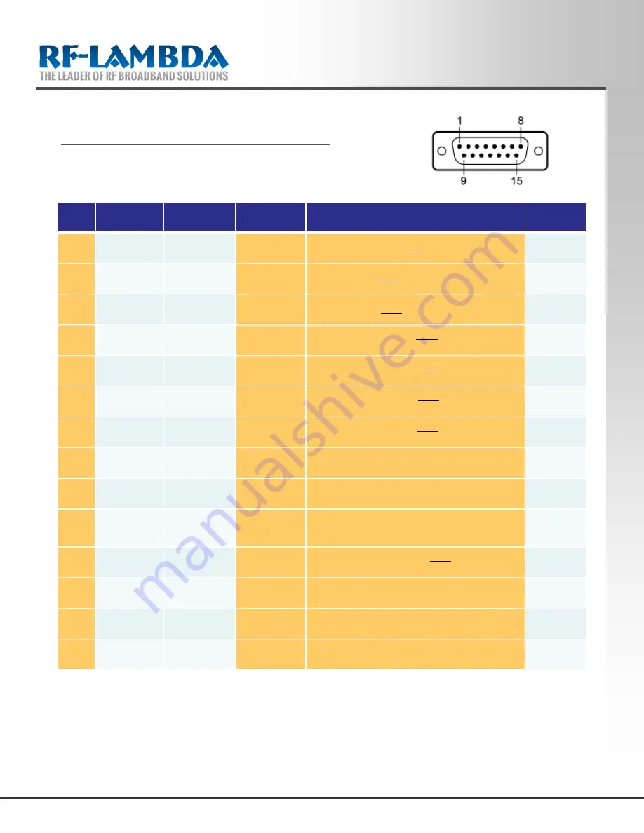
User Control Connector on Rear Panel 

HIGH/LOW voltages are standard TTL signals:

0.0V-0.8V = LOW

2V-5V = HIGH 

Summary of Contents for RAMP02G06GC

Page 1: ...easurement Research and Development Parameter Min Typ Max Min Typ Max Units Frequency Range 2 4 4 6 GHz Gain 75 65 dB Gain Flatness 5 4 dB Gain Variation Over Temperature 45 85 3 3 dB Input Return Loss 7 7 dB Output Return Loss 10 10 dB Saturated Output Power Psat 50 50 dBm IM3 30 30 dBc Output Third Order Intercept IP3 dBm Isolation S12 65 65 dB Supply Current 110V 220V AC Quiescent 1 8 Max 10 A ...

Page 2: ... output Power OFF Procedure Step 1 Turn off RF output power Step 2 Turn Off AC power Step 3 Disconnect input and output Environmental Specifications and Test Standards Parameter Description Operational Temperature 45 85 Case Temperature Storage Temperature 55 125 Thermal Shock 45 85 5 Cycles 10 hours Random Vibration MIL STD 202G Table 214 I Test Condition Letter C 1 5 Hours Per Axis High Temperat...

Page 3: ...eration with poor loads is discouraged If prolonged operation with poor or unknown loads is expected an external device such as an isolator or circulator should be used to protect the amplifier Ensure that the power is off when connecting or disconnecting the input or output of the amp Prevent overdriving the amplifier Do not exceed the recommended input power level Adequate heat sinking required ...

Page 4: ...echnical support rflambda com RAMP02G06GC 100W Wide Band Solid State EMC Benchtop Power Amplifier 2 6GHz Rev 2 03 19 2021 Small Signal S Parameters Note Input output return loss measurements include attenuators to protect equipment Typical Performance Plots ...

Page 5: ...02G06GC 100W Wide Band Solid State EMC Benchtop Power Amplifier 2 6GHz Rev 2 03 19 2021 Gain vs Output Power 2 1 and 5 9GHz P7dB vs Frequency 2 1 and 5 9GHz Gain vs Output Power 2 2 and 5 8GHz P7dB vs Frequency 2 2 and 5 8 GHz Gain vs Output Power 2GHz to 6GHz P7dB vs Frequency 2GHz to 6GHz ...

Page 6: ... sales rflambda com Technical support rflambda com RAMP02G06GC 100W Wide Band Solid State EMC Benchtop Power Amplifier 2 6GHz Rev 2 03 19 2021 2nd Harmonic Wave vs Pout 3rd Harmonic Wave vs Pout 4th Harmonic Wave vs Pout Current vs Pout ...

Page 7: ... any of the information contained herein RF Lambda assumes no responsibility or liability whatsoever for the use of the information contained herein The information contained herein is provided AS IS WHERE IS and with all faults and the entire risk associated with such information is entirely with the user All information contained herein is subject to change without notice Customers should obtain...

Page 8: ...9 2021 Power Indicator Gain Adjustment Knob ON OFF switch Instrument AC power supply switch USER CONTROL D SUB Connector low voltage 3 3V TTL control signals See page below for more information Front Panel Rear Panel RF Output RF Input Alarm Indicator Keypad Fuse Holder USB Port upon request LAN Port upon request Main AC connector GND connector EMC Equipment User Manual ...

Page 9: ...o eliminate the error code press RESET on front panel keypad to reboot the instrument and clear the alarms If error code can not be eliminated after reboot please contact support rflambda com Calibration is may be recommended 1 Calibrate to execute instrument self calibration process 2 Reset to reboot the instrument Please turn OFF RF input power and terminate the RF output port while applying cal...

Page 10: ...ction Selection Page Instrument Status Display Page To enter this function selection page press Menu on front panel keypad while the instrument is showing the status page Press the corresponding number on front panel keypad to select 1 Calibrate calibrates the instruments 2 Frequency enters RF input signal center frequency 3 RF ON OFF switches the RF output port on or off 4 Reset Restarts the inst...

Page 11: ...er is driven over temperature Yes 6 Current Over Indicator LOW Pin will be latched to logic HIGH when drain current limit is reached Yes 7 ID Imbalance Indicator LOW Pin will be latched to logic HIGH when an imbalance in the drain current of the combining branches occurs Yes 8 PA input power Indicator PA input power is represented by voltage No 9 PA output power Indicator PA output power is repres...

Reviews: