R12UZ0080EU0102 Rev.1.02
Page 4
Apr 1, 2022
ISL9122AIIN-EVZ, ISL9122AIRN-EVZ Evaluation Board Manual
1.2
Setup and Configuration
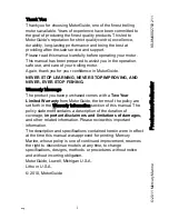
For both evaluation boards, the default output voltage is set at 3.3V. Use the following procedures to configure
and power-up the board for proper operation. During the power-on process, the expected waveforms are shown in
.
1. Connect the power supply to J1, with voltage setting between 1.8V and 5.5V.
2. Connect the electronic load to J2.
3. Place the scope probes on VOUT test point and other test points of interest.
4. Ensure that the EN pin jumper (J4) is pulled up to V
IN
.
5. Turn on the power supply. At the end of the soft start sequence, the ISL9122A is operating in Regulation mode
by default with V
OUT
= 3.3V.
Note
: A minimum effective output capacitance of 6µF is required. Therefore,
depending on the performance specifications of the capacitor, an additional output capacitor might be required
for higher output voltage settings.
6. Monitor the output voltage start-up sequence on the scope. The waveforms should look similar to those shown
.
7. Turn on the electronic load.
8. Measure the output voltage with the voltmeter. The voltage should regulate within the datasheet specification
limits.
9. To determine efficiency, measure input and output voltages at the Kelvin sense test points (S+ and S-), which
are part of J1 and J2 headers. The bench power supply can be connected to the VIN and GND headers on J1.
The electronic load can be connected to the VOUT and GND headers on J2. Measure the input and output
currents. Calculate the efficiency based on these measurements.
1.3
Evaluation Software Installation and Use
The ISL9122 evaluation software and evaluation software guide are available for download from the Renesas
.
10. Save the evaluation software executable file and install the evaluation software (refer to the evaluation software
manual). When the evaluation software launches, (refer to the
supply, DC load, and other test equipment to the evaluation board; next, apply power.
11. The ISL9122A has five control registers. See the ISL9122 datasheet for detailed register descriptions.
12. Register
RO_REG1
(Address: 0x02) provides chip identification information. The
Get IC INFO_RO_REG1
button reads from this read-only register.
13. To change the output voltage, you can use the
VSET Control
slider in the
VSET
register (Address: 0x11) panel
and perform a Write REG operation. The output voltage ramps up at the slew rate specified in the
DVSRATE
Figure 3. ISL9122A Start-Up with V
IN
= 3.6V and V
OUT
= 3.3V
200
μ
s
/Div