


ClockMatrix
EEPROM Programming Instructions
Feb.10.20
Page 2 of 7
1.
EEPROM Overview
The ClockMatrix 8A3xxxx product family from Renesas is designed to power-up and operate using internal
resources. However, there may be cases where it is necessary or convenient to use an external I2C serial
EEPROM for the device in order to obtain alternate information at reset.
The external EEPROM can be used to contain one or more of the following:
• Device configuration information block (Config)
• Micro-controller Firmware Full Application Load (FW Application)
• Micro-controller Firmware Patch (FW Hotfix)
These blocks may appear in any order in the EEPROM, but only one FW Application or one FW Hotfix will be
applied. A FW Hotfix may not be applied to a FW Application block loaded from EEPROM; only to the internal
(embedded) firmware. Any number of Config blocks are allowed.
Renesas will provide the EEPROM image in the form of a .hex file that is formatted according to the Intel Hex
format. Details of the structure of the EEPROM is beyond the scope of this document.
The following instructions describe the hardware connections for the EEPROM, how to program the EEPROM
using the Clock Matrix chip, and other miscellaneous information.
2.
Hardware Setup
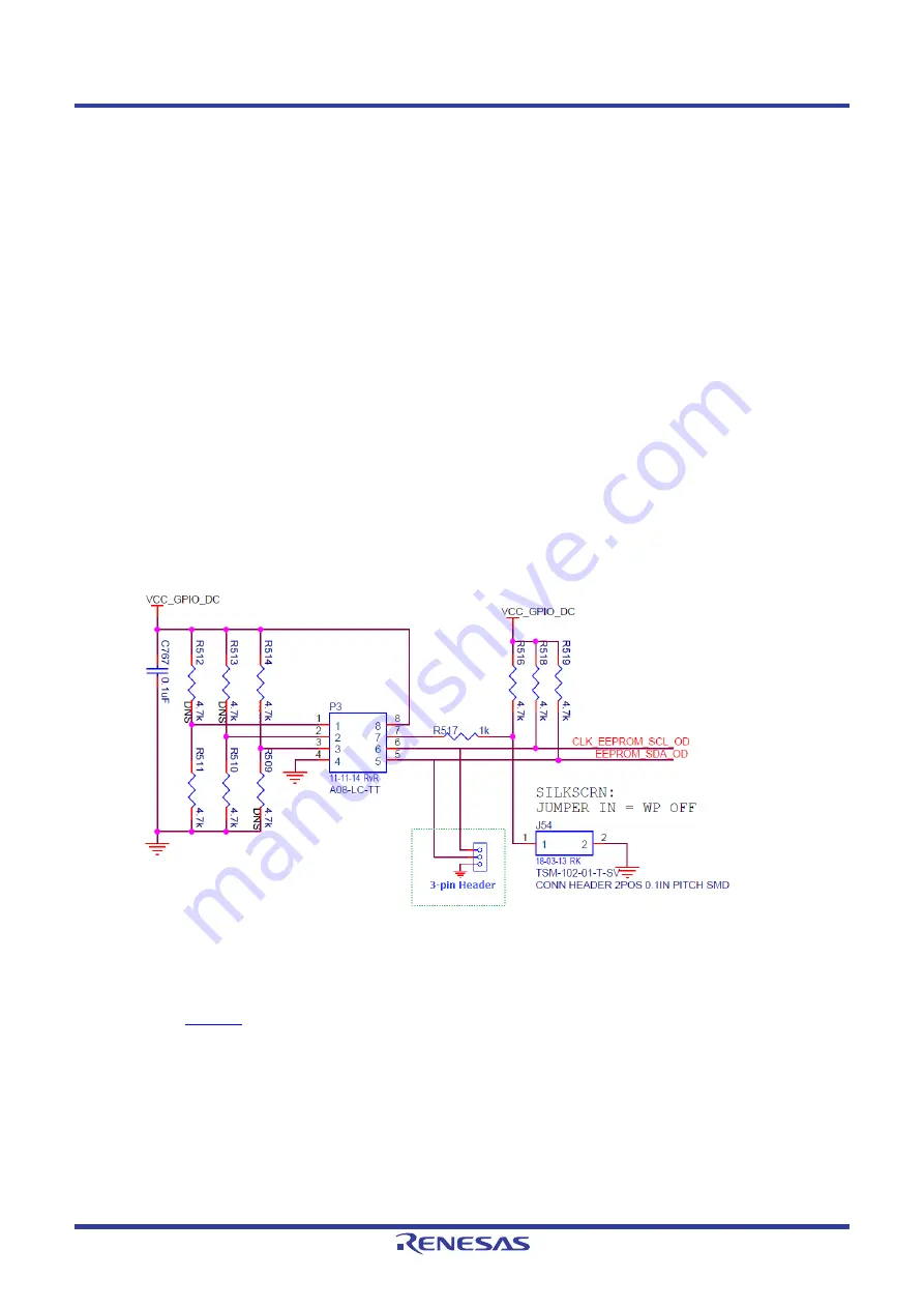
The following is an example setup schematic.
Figure 1. EEPROM Circuit
Connect the SCLK and SDA traces to the ClockMatrix device master I2C port (SCLK and SDA). Another
recommendation is to also place a 3-pin header that connects to the EEPROM SCLK, SDA, and GND pin (see
green outline in
). Using this method, an external programmer can be connected to the system for
programming. Be aware that external programmers may only support 3.3V levels, so if the VCC_GPIO on the
chip is 1.8V or 2.5V a level translator is required.