background image

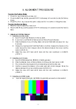
4. ALIGNMENT PROCEDURE 


To enter the Factory Mode 

1.  Press Vol.- key to reduce the volume to 0. 

2.  Press the MUTE key and the password “9735” continuously in 5 seconds to enter the Factory 

Mode. 

3.  Press Pro.-/Pro.+ key to select the option, and press Vol.+ to confirm or change the value. 

To enter the Service Menu 

1.  Press Vol.- key to reduce the volume to 0. 

2.  Press the MUTE key and the password “3175” continuously in 5 seconds to enter the Service 

Menu. 


1. 

Adjustment of White Balance: 

1)  Adjustment in VGA mode: 

A.  Input 11 Gray Scales Patten from Chroma 2225. 

B.  In user menu, set Warmth to Normal and set Picture Preset to Natural. 

C.  Enter the Balance menu in Factory Mode, and select VGAcalbr and press Vol.+ key 

to activate. 

D.  Change the input signal to Full White Pattern. And then measure the balance in the 

center area with a Color Analyzer. (Note: the distance between the screen and the 

sensor is 25-30 cm ) 

E.  Adjust the value of R Gain and B Gain until the color coordinate is x=299±15, 

y=215±15. 


2)  Adjustment in TV mode: 

A.  Input Full White signal from PM5418 or 54200 generator. 

B.  Enter the Balance menu of Factory Mode, and change the input source to VID. 

C.  Then connect the input signal to the corresponding port with a video wire. 

D.  And then measure the balance in the center area with a Color Analyzer. (Note: the 

distance between the screen and the sensor is 25-30 cm ) 

E.  Adjust the value of R Gain and B Gain until the color coordinate is x=285±15, 

y=294±15. 


3)  Adjustment in YPbPr mode: 

A. 

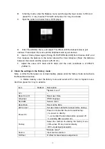
Input the signal (Timing 35, PATTERN 36 and 480I) as below from Chroma2327. 


14

Summary of Contents for LCD37V6SY

Page 1: ...ist 7 4 Alignment Procedure 14 5 Schematic Diagram 17 6 Explode View Diagram Absence temporarily 34 This manual is the latest at the time of printing and does not include the modification which may be made after the printing by the constant improvement of product ...

Page 2: ...lectric shock to the person The exclamation point within an equilateral triangle is intended to alert the user to the presence of important operating and maintenance servicing instructions in the literature accompanying the appliance CAUTION Use of controls adjustments or procedures other than those specified herein may result in hazardous radiation exposure CA U T ION RISK RISK OF ELECTRI ELECTRI...

Page 3: ...o impact of any kind Be particularly careful not to damage the picture tube surface 9 Unplug this television set from the wall outlet before cleaning Do not use liquid cleaners or aerosol cleaners Use a damp cloth for cleaning 10 1 Do not place this television set on an unstable cart stand or table The television set may fall causing serious injury to a child or an adult and serious damage to the ...

Page 4: ...ing conductors location of antenna discharge unit connection to grounding electrode and requirements for the grounding electrode 15 2 Note to CATV system installer Only for the television set with CATV reception This reminder is provided to call the CATV system attention to Article 820 40 of the NEC that provides guidelines for proper grounding and in particular specifies that the cable ground sha...

Page 5: ...edurein youroperatinginstructions do not attempt any further adjustment Unplug the set and call your dealer or service technician 22 Whenever the television set is damaged or fails or a distinct change in performance indicates a need for service unplug the set and have it checked by a professional service technician 23 It is normal for some TV sets to make occasional snapping or popping sounds par...

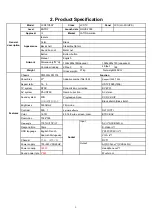
Page 6: ...Dynamic skin correction DVI PC AV system PAL NTSC Gama correction AV stereo Sound system M N Progressive Scan CCD V CHIP MONO BTSC SAP Black stretch Blue stretch Brightness 500Cd m2 Film mode Contrast 500 1 4 picture effects DLTI DCTI Color 16 7M 4 3 16 9 wide screen zoom BTSC SAP Resolution 1366 768 View angle 176 H 176 V AV in 3 CVBS R L Respond time 16ms S Video in 1 OSD language English French...

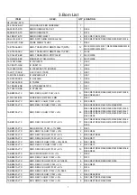
Page 7: ... 5 2 R576 R575 19 BB0101 JTX SMD RES 100 OHM 1 10W 5 7 R600 R599 R522 R641 R519 R508 R507 19 BB0102 JTX SMD RES 1K OHM 1 10W 5 26 R663 R664 R568 R562 R559 R554 R551 R550 R546 R539 R538 R535 R533 R527 R630 R631 R509 R515 R516 R517 R518 R520 R521 R644 R645 R558 19 BB0103 JTX SMD RES 10K OHM 1 10W 5 17 R557 R633 R632 R506 R510 R532 R541 R544 R549 R567 R569 R616 R615 R570 R574 R597 R598 19 BB0123 FTX ...

Page 8: ...28 BB0105 ZFX SMD CAP 1UF 50V 80 20 1 C594 28 BB0152 KBX SMD CAP 0 0015UF 50V B 0805 1 C523 28 BB0224 ZFX SMD CAP 0 22UF 50V 80 20 0805 11 C502 C503 C501 C500 C625 C599 C596 C591 C590 C585 C584 28 BB0339 CCX SMD CAP 3 3PF 50V 0 25PF 2 C512 C511 28 BB0471 JCX SMD CAP 470PF 50V 5 1 C521 28 BB0474 ZFX SMD CAP 0 47UF 50V 80 20 2 C586 C592 28 BB0560 JCX SMD CAP 56PF 50V 5 2 C510 C508 28 BB0820 JCX SMD ...

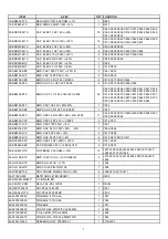
Page 9: ...C AIC1084 33CM 3 3V TO 263 1 U014 13 IRF731 40B IC IRF7314 1 U004 13 LD1117 33B IC LD1117 3 3V 1 U007 13 M24C32 MNB IC SM M24C32 WMN6P ST00 R 1 U021 13 PT7809 STB IC PT7M7809ST 1 U09 13 PW1181 0LB DEINTERLACER AND SCALER PW118 10 1 U002 13 PW3300 10B IC PW3300 10 1 U008 13 SRV054 CTB IC SRV05 4 TCT 2 D001 D005 13 AL008D 70BT2 FLASH 8M S29AL008D70TFI02 1 U020 19 AB0000 JTX RES SMD 0 OHM 1 10W 5 060...

Page 10: ...4 RP003 RP002 RP001 28 AB0102 JCX SMD CAP 1000PF 50V 5 0603 5 C215 C164 C191 C184 C176 28 AB0103 ZFX CAP SMD 10NF 50V 80 20 0603 2 C019 C018 28 AB0104 ZFX CAP SMD 0 1UF 50V 80 20 F 1 C216 28 AB0120 JCX SMD CAP 12 PF 50VDC 0603 5 3 C180 C179 C178 28 AB0180 JCX SMD CAP 18 PF 50V 5 0603 8 C158 C202 C201 C083 C084 C085 C200 C157 28 AB0224 ZFX CAP SMD 0 22UF 50V 80 20 0603 6 C173 C174 C177 C187 C192 C1...

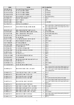
Page 11: ...K3 3 5 3WK E 1 J002 47 RCA009 XX4 RCA SOCKET AV 3 2 3W 052 1 J006 47 RCA123 XX0 RCA SOCKET AV 3 2 2W G6 2 J004 J003 47 RCA125 XX1 RCA SOCKET AV 3 2 3W 051 1 J007 47 VGA004 XX0 VGA SOCKET D SUB 15S BLACK 1 P004 67 387190 0A0 HEAT SINK 1 FOR U002 67 387190 1A0 HEAT SINK 2 FOR U012 FOR U013 67 H42094 0A0 HEAT SINK 1 FOR U008 19 AB0751 FTX SMD RES 750 OHM 1 10W 1 1 R111 T8 37V6AY EAY ASS Y EARPHONEBD ...

Page 12: ...M 1 10W 5 1 R704 19 BB0221 JTX SMD RES 220 OHM 1 10W 5 0805 2 R713 R705 19 BB0223 JTX SMD RES 22K OHM 1 10W 5 3 R701 R702 R706 19 BB0303 FTX RES SMD 30K 0HM 1 10W 1 1 R716 19 BB0331 JTX SMD RES 330 OHM 1 10W 5 0805 1 R708 19 BB0471 JTX SMD RES 470 OHM 1 10W 5 1 R703 25 BCB101 M1X CAP ELEC 100 UF 16V 20 4 C716 C718 C702 C710 25 BFB220 M1X CAP ELEC 22 UF 50V 20 1 C713 25 BFB470 M1X CAP ELEC 47 UF 50...

Page 13: ...5490 0HC1B DECORATE BAR 1 46 40019H 30X LVDS 19CM 3Y 1 46 KF080F 12X01 INVERTER Y0509142 2 1 81 LC32A7 PW1 32 SMPS JSK3220 007A 1 T8 37V6AY MTY ASS Y METAL 1 T8 37V6AY PAN PACKING ASSEMBLY 1 T8 37V6AY PANZ ASS Y ARFPACKINGPARTS 1 72 26V6SY E001A OPERATION MANUAL 1 06 015W33 A003X REMOTE CONTROLLER RC1113323 1 51 PC0220 0YU08 POWER CORD 1 T8 37V6AY RCN REAR CABINET ASSEMBLY 1 T8 37V6AY BSY ASS Y BA...

Page 14: ...lbr and press Vol key to activate D Change the input signal to Full White Pattern And then measure the balance in the center area with a Color Analyzer Note the distance between the screen and the sensor is 25 30 cm E Adjust the value of R Gain and B Gain until the color coordinate is x 299 15 y 215 15 2 Adjustment in TV mode A Input Full White signal from PM5418 or 54200 generator B Enter the Bal...

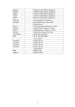
Page 15: ...4 15 2 Check the settings in the Factory mode Note a After the first power on or downloading please enter the factory mode and activate the Reset Data function b Before delivery enter the factory menu and select All For User in System menu And then press Vol key to activate Item Default Description System menu GM Reset User D Reset user Data Language OSD Language ServiceM Service menu Reset Data R...

Page 16: ...e YUVcalbr Color calibration for other sources TvGeom menu TvHPos Horizontal position of image in TV mode TvHsize Horizontal size of image in TV mode TvVPos Vertical position of image in TV mode TvVSize Vertical size of image in TV mode Clear Screen Not be used temporarily Shift Not be used temporarily Sound menu CurveP1P Sound curve X1 CurveP1V Sound curve Y1 CurveP2P Sound curve X2 CurveP1V Soun...

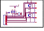
Page 17: ...706 47P R713 220 L703 100uH R707 10K R716 27K 1 R708 330 1k NS R717 U701 RT34063 1 2 3 4 5 6 7 8 SC SE TC GND COMP VCC IPK DRIVER C708 100U 16V C702 47U 16V R718 100 L704 100UH C701 0 1U C703 100U 16V Q702 SOT 23 R711 100 Q701 SOT 23 C713 22u 50v LN9 220UH C704 470U 16V C718 100uF 16V R703 1 3K R712 100 C707 103 R714 1 1 R705 220 C705 47P R715 1K 1 L705 33R FB TUN4 07 389FI5 NX0 18 17 16 15 14 13 ...

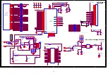
Page 18: ...20u 25V CE 8S C596 0 22u C 0805 C636 100uF 10V R508 100 R544 10K R517 1K C557 0 1u C 0805 C544 470u 16v J508 2 3 1 4 C542 104 R558 1K D512 1N5817 D 4148S L514 10uH Q517 3904 L504 10uH C545 470u 16v Q514 3904 R520 1K R595 220 R565 8 2k 1 C625 0 22u C 0805 R514 51K 1 C589 220u 25V CE 8S C635 0 1uF 47 RCA013 XX2 1 2 C600 100u 16v C546 470u 16v C586 0 47uF C 0805 R592 680 C611 82pF C632 100uF 10V R516...

Page 19: ...5 0 A 19 1 ROMWEn SCL SDA Page 4 04_HDTVIN HDCR1 HDY1 HDCB1 HDSOG1 Page 13 13_DISPLAY DPWON PWM2 LVDSON Page 11 11_MISC ROMWEn ROMOEn A 19 1 D 15 0 SDA SCL DPWON PWRON RESETn MUTE GRXD GTXD SW1 SW2 AFT KEY1 IR LED OUT P_ON PWM2 KEY2 LVDSON SMXJ DIPB OE CONTRAL Page 15 15_PW2300PWR Page 17 17_REVISION Page 6 06_GINPUT RAIN GAIN BAIN VSYNC HSYNC PCSOG GRXD GTXD Page 12 12_MAIN_MEMORY Page 10 10_INPO...

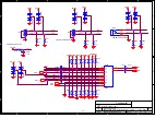
Page 20: ... 1uF L001 FB_1K_OHM_200MA R010 26 7 R009 26 7 C002 0 1uF C001 0 1uF C006 0 1uF R013 26 7 R008 4 75K R012 26 7 C008 0 1uF D005 srv05 4 1 3 2 4 5 6 P001 DVI_V 1 2 3 4 5 6 7 8 9 10 11 12 13 14 15 16 17 18 19 20 21 22 23 24 33 34 25 26 27 28 29 30 31 32 DATA2 DATA2 DATA2 4_SHLD DATA4 DATA4 DDC_CLK DDC_DATA A_VSYNC DATA1 DATA1 DATA1 3_SHLD DATA3 DATA3 5V GND H_PLUG_DET DATA0 DATA0 DATA0 5_SHLD DATA5 DA...

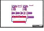
Page 21: ...02 DF14A 30P 1 25H 1 2 3 4 6 8 10 12 14 16 18 20 22 24 26 28 30 7 9 11 13 15 17 19 21 23 25 27 29 5 Q001 NC 1 2 3 C033 22uF 16V RP007 47R 1 8 2 3 4 5 6 7 R177 0 RP005 47R 1 8 2 3 4 5 6 7 C016 0 1uF RP011 47R 1 8 2 3 4 5 6 7 R178 0 L005 33R FB Q002 DTC144EKA 1 2 3 C019 0 01uF C029 0 1uF R021 nc R179 0 R025 6 8K R038 NC R030 0 R031 1K C014 0 1uF R180 0 R029 4 7K P003 CONN PCB 7 1 2 3 4 5 6 7 1 2 3 4...

Page 22: ...C036 10uf 1 2 R046 22k R043 47k C041 10uf 1 2 R045 47k R055 22k R044 47k D011 BAV99L 1 3 2 L009 25uH D009 BAV99L 1 3 2 R040 47k D010 BAV99L 1 3 2 D008 BAV99L 1 3 2 D006 BAV99L 1 3 2 R048 22k D023 BAV99L 1 3 2 C045 10uf 1 2 D007 BAV99L 1 3 2 R054 22k J003 CONNECTOR COAX J 1 2 3 4 R052 22k D024 BAV99L 1 3 2 R053 22k R049 22k C038 10uf 1 2 R051 22k C039 10uf 1 2 U005 4052 12 14 15 11 1 5 2 4 6 10 9 1...

Page 23: ... M5 M4 J7 K9 K7 L9 K6 K5 K4 K8 J8 J1 J2 J3 J4 M8 M7 M9 G8 G7 E7 F7 E5 F5 G6 E4 F4 G5 G4 H4 H1 H2 H3 H5 J5 J6 H8 H7 H6 E6 E9 F6 E8 F8 E11 E12 G12 J12 L10 L12 F10 G10 H10 J10 K10 D10 D11 D12 D13 E13 F13 G13 H13 J13 K13 L13 M10 M11 M12 E10 F12 F11 F9 G11 G9 H11 H12 H9 J11 K11 K12 L11 J9 V33ADC1 V33ADC2 V33ADC3 V33ADC4 V33ADC5 V33ADC6 V33ADC7 V33ADC8 GND2 GND3 GND5 GND6 GND7 GND8 GND9 GND4 GND1 V18A2 ...

Page 24: ...10 R071 NC R068 0 C085 18pF R086 0 IIC1 CON4 1 2 3 4 R092 1 00K R088 0 TP002 R069 NC R075 47 Y001XTAL14 31818 1 2 R076 10 0K U09 PT7M7809 1 2 3 1 2 3 Misc U002D PW118 D12 B12 A10 C12 D11 E12 C11 C8 A11 C9 C10 D8 D7 B8 C7 B11 D9 A7 D10 B17 D14 D17 C17 D16 D15 C14 C15 A16 C16 B15 B16 D13 B14 A14 A15 A12 A9 B9 A13 C13 B13 Y8 AA8 Y13 W13 AB13 AA13 Y9 AB11 AA10 AA9 AB12 AB10 W9 W10 Y10 W11 AA11 AA12 AB...

Page 25: ...1547R 1 8 2 3 4 5 6 7 Input Port 1 U002B PW118 AA4 Y1 W4 W1 AB5 W2 AA5 AA3 V3 R1 AB3 R2 T2 T1 V4 AA2 R3 Y2 U2 V1 P4 U4 V2 W5 U3 R4 Y4 AB6 AA1 AB1 W3 AB2 Y3 P5 T4 Y5 U1 AB4 T3 IN1R0 IN1R1 IN1R2 IN1R3 IN1R4 IN1R5 IN1R6 IN1R7 IN1G0 IN1G1 IN1G2 IN1G3 IN1G4 IN1G5 IN1G6 IN1G7 IN1B0 IN1B1 IN1B2 IN1B3 IN1B4 IN1B5 IN1B6 IN1B7 IN1CLK IN1PEN IN1VBI IN1HS IN1AHS IN1CST IN1CMP IN1VS IN1FLD IN1B8 IN1B9 IN1G8 IN...

Page 26: ...E ECN NUMBER REV DESCRIPTION OF CHANGE Initial release 00 A 5 5 04 NA 900 0254 00 Trinity Production Reference Design A Revision History B 8 15 Monday October 25 2004 Variant Name Title Size Document Number Rev Date Sheet of Confidential 26 ...

Page 27: ... VSS1 VSSQ1 VSSQ2 VSSQ5 VSSQ4 VSSQ3 LDQS VDD2 VDD3 LDM WE CAS RAS CS BA0 BA1 A10 AP A0 A1 A2 A3 A4 A5 A6 A7 A8 A9 A11 A12 CKE CK CK UDM VREF UDQS RP017 22R 1 8 2 3 4 5 6 7 RP020 22R 1 8 2 3 4 5 6 7 RP024 22R 1 8 2 3 4 5 6 7 RP032 22R 1 8 2 3 4 5 6 7 Main Memory Port U002F PW118 M22 C22 G22 L20 L19 J21 E22 B19 J20 F22 K19 K20 A20 G21 K18 M18 H22 V22 U21 U20 T19 A18 B20 A19 A17 B18 N22 N21 E20 D20 T...

Page 28: ...2 N13 N14 N19 P9 P10 P11 P12 P13 P14 U18 V8 W6 W8 A21 C18 E13 E14 E15 E17 F17 F18 F20 G18 H18 H21 J18 R5 J19 J22 N18 P18 P20 R18 T18 U22 E10 E11 E16 F6 E7 E8 H5 J5 T5 U17 V11 V12 V13 L18 M5 Y7 AA7 U5 N5 V9 V10 V15 V16 J12 J9 J10 U19 GND1 GND4 GND6 GND7 GND8 GND9 GND10 GND11 GND12 GND13 GND14 GND15 GND16 GND17 GND18 GND19 GND20 GND21 GND22 GND23 GND24 GND25 GND26 GND27 GND28 GND29 GND30 GND31 GND32...

Page 29: ...6 M15 M14 M13 N16 N15 N14 P16 P15 P14 R16 R15 R14 T16 T15 T14 T13 B9 D9 A8 B8 C8 D8 A7 C5 D5 FILT DGCLK1 DGPEN DGAHS DGHS DGVS DGFLD ASPECT0 ASPECT1 ASPECT2 RXCP RXCM RX0P RX0M RX1P RX1M RX2P RX2M RTERM RED1 RED2 RED3 RED4 GRN1 GRN2 GRN3 GRN4 BLU1 BLU2 BLU3 BLU4 SOG1 SOG2 SOG3 SOG4 HS1 HS2 VS1 VS2 R2 G2 B2 S2 REXT DGCLK2 DGRE0 DGRE1 DGRE2 DGRE3 DGRE4 DGRE5 DGRE6 DGRE7 DGGE0 DGGE1 DGGE2 DGGE3 DGGE4...

Page 30: ... 7 8 NC1 NC2 NC3 GND SDA SCL VCLK VCC R146 2 21K D016 BAV99L 1 3 2 L028 FB_11_OHM_500MA U019A 74ACT08A 1 2 3 7 14 C176 1nF R150 3 32K D012 BAV70L 1 2 3 D019 BAV99L 1 3 2 C179 12pF D017 BAV99L 1 3 2 R159 0 C172 0 1uF C175 0 1uF R147 2 21K L025 FB_11_OHM_500MA R156 75 C173 0 18uF U019D 74ACT08A 13 12 11 U019C 74ACT08A 10 9 8 U019B 74ACT08A 4 5 6 D018 BAV99L 1 3 2 C180 12pF R148 4 75K R155 75 R145 4 ...

Page 31: ...33 V33 V33 V33 R162 nc R166 10 0K JP006 HDR_4X1 1 2 3 4 JP004 HDR_RA 25x2 1 2 3 4 5 6 7 8 9 10 11 12 13 14 15 16 17 18 19 20 21 22 23 24 25 26 27 28 29 30 31 32 33 34 35 36 37 38 39 40 41 42 43 44 45 46 47 48 49 50 R167 10 0K JP005 HDR_2X1 1 2 R164 2 00K C183 0 1uF R161 nc R160 1 00K SW3 SW_DPDT_SMT 3 2 1 4 5 6 U021 24LC32A 5 6 8 4 1 2 3 7 SDA SCL VCC GND NC0 NC1 NC2 WP C181 0 1uF R165 10 0K C182 ...

Page 32: ... C204 470pF FID24 1 R169 75 FID52 1 FID11 1 FID51 1 FID26 1 C184 1nF FID43 1 FID34 1 R187 75 J006 CONNECTOR COAX J 1 2 3 4 5 6 FID25 1 C186 0 1uF FID56 1 FID12 1 FID50 1 FID27 1 FID57 1 C209 47pF C206 47pF FID35 1 L39 10nH FID54 1 FID41 1 FID44 1 FID13 1 FID36 1 FID28 1 FID38 1 FID19 1 FID42 1 C185 0 1uF FID14 1 C207 270pF FID29 1 C205 12pF FID20 1 FID55 1 R192 40 2 J005 CON64 1 2 3 4 5 6 7 8 9 10...

Page 33: ...C HD1CBL HD1S HD1CRC HD1CRL HD1CR HD1CBF HD1CRF VCCG VCCG VCCG L036 330nH L304 470nH C190 56pF C194 82pF L038 56nH C192 0 18uF D020 BAV99L 1 3 2 C197 150pF R170 75 R172 75 L030 330nH C195 56pF L037 470nH J007 CONNECTOR COAX J 1 2 3 4 5 6 C198 82pF L032 56nH C196 0 18uF L031 470nH C188 150pF L033 330nH R173 75 D021 BAV99L 1 3 2 C191 1nF C199 56pF R171 3 32K C189 82pF C193 150pF L035 56nH C187 0 18u...

Reviews: