Smart LTE Module Series
SC66 Hardware Design
SC66_Hardware_Design 69 / 139
3.18. LCM Interfaces
SC66 video output interface (LCM interface) is based on MIPI_DSI standard and supports 8 groups of
high-speed differential data transmission and WQXGA display (resolution: 2560 × 1600), Support dual
display, default DSI+DP (Type-C), optional DSI0+DSI1. Note that DSI1 does not support screens with
command mode.
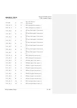
Table 25: Pin Definition of LCM Interfaces
Pin Name
Pin No.
I/O
Description
Comment
LDO11A_1P8
10
PO
1.8V output power supply
for LCM logic circuit and
DSI
LDO3B_2P8
12
PO
2.8V output power supply
for LCM analog circuits
PWM
152
DO
PWM signal output
Cannot be multiplexed into
a general-purpose GPIO.
LCD0_RST
127
DO
LCD0 reset signal
It should not be pulled up.
LCD0_TE
126
DI
LCD0 tearing effect signal
DSI0_CLK_N
116
AO
LCD0 MIPI clock signal (
-
)
DSI0_CLK_P
115
AO
LCD0 MIPI clock signal
(
+
)
DSI0_LN0_N
118
AO
LCD0 MIPI lane 0 data
signal (
-
)
DSI0_LN0_P
117
AO
LCD0 MIPI lane 0 data
signal (
+
)
DSI0_LN1_N
120
AO
LCD0 MIPI lane 1 data
signal (
-
)
DSI0_LN1_P
119
AO
LCD0 MIPI lane 1 data
signal (
+
)
DSI0_LN2_N
122
AO
LCD0 MIPI lane 2 data

