background image

UMTS/HSPA+/LTE Standard Module Series 

Mini  PCIe-C  EVB  User  Guide


Mini_PCIe-C_EVB_User_Guide                                                                                                                  27 / 39 


4.5. UART Interface (J301) 


The UART interface of the Mini PCIe-C EVB is intended for the communication between the module and 

the host application. It can be used for data transmission and AT command communication. 


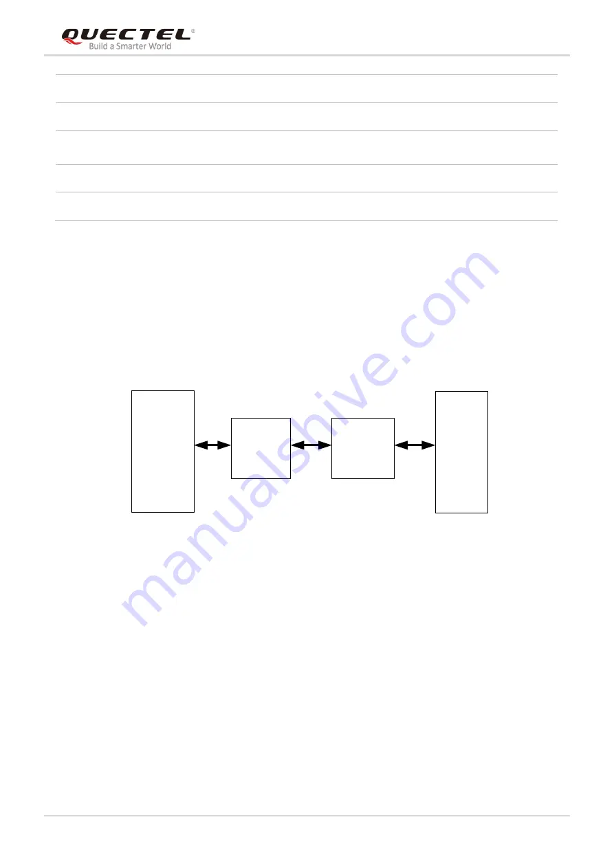
The following figure shows the block diagram of the UART interface on Mini PCIe-C EVB. 


RS232 

Level Match

Level 

Translator

COM

DB9

J301

RS232 

3.0V 

 1.8V

J101

U

A

R

T

 in

te

rfa

ce


Figure 23: Block Diagram of UART Interface 


C5 

GND 

Ground 

C6 

VPP 

Not connected 

C7 

SIM_DATA 

I/O 

Data line.   

Bidirectional 

CD1 


Not connected 

CD2 


Not connected 

Summary of Contents for Mini PCIe-C EVB

Page 1: ...Mini PCIe C EVB User Guide UMTS HSPA LTE Standard Module Series Rev Mini_PCIe C_EVB_User_Guide_V1 0 Date 2019 11 08 Status Released www quectel com ...

Page 2: ...TS CUSTOMERS THE INFORMATION PROVIDED IS BASED UPON CUSTOMERS REQUIREMENTS QUECTEL MAKES EVERY EFFORT TO ENSURE THE QUALITY OF THE INFORMATION IT MAKES AVAILABLE QUECTEL DOES NOT MAKE ANY WARRANTY AS TO THE INFORMATION CONTAINED HEREIN AND DOES NOT ACCEPT ANY LIABILITY FOR ANY INJURY LOSS OR DAMAGE OF ANY KIND INCURRED BY USE OF OR RELIANCE UPON THE INFORMATION ALL INFORMATION SUPPLIED HEREIN IS S...

Page 3: ...UMTS HSPA LTE Standard Module Series Mini PCIe C EVB User Guide Mini_PCIe C_EVB_User_Guide 2 39 About the Document History Revision Date Author Description 1 0 2019 11 08 Jouni YANG Woody WU Initial ...

Page 4: ... 4 3 1 1 Earphone Interface J401 19 4 3 1 2 Handset Interface J404 21 4 3 2 Analog Audio Interfaces J402 J403 22 4 3 2 1 Handset Interface J402 22 4 3 2 2 Earphone Interface J403 24 4 4 U SIM Interface J303 25 4 5 UART Interface J301 27 4 6 Switch and Button S201 S101 29 4 7 Status Indicators D103 D101 30 4 8 Test Points 31 5 Operation Procedures Illustration 33 5 1 Turn on the Mini PCIe C D and E...

Page 5: ...3 TABLE 4 PIN DEFINITION OF J302 18 TABLE 5 PIN DEFINITION OF J401 20 TABLE 6 PIN DEFINITION OF J404 22 TABLE 7 PIN DEFINITION OF J402 23 TABLE 8 PIN DEFINITION OF J403 25 TABLE 9 PIN DEFINITION OF J303 26 TABLE 10 PIN DEFINITION OF J301 28 TABLE 11 DESCRIPTION OF S201 AND S101 29 TABLE 12 DESCRIPTION OF D103 AND D101 30 TABLE 13 DESCRIPTION OF TEST POINTS 31 TABLE 14 RELATED DOCUMENTS 38 TABLE 15...

Page 6: ...CIRCUIT DESIGN FOR HANDSET INTERFACE J402 22 FIGURE 17 PIN ASSIGNMENTS OF HANDSET INTERFACE J402 23 FIGURE 18 REFERENCE CIRCUIT DESIGN FOR EARPHONE INTERFACE J403 24 FIGURE 19 PIN ASSIGNMENTS OF EARPHONE INTERFACE J403 24 FIGURE 20 SKETCH DESIGN OF CTIA AUDIO PLUG 25 FIGURE 21 REFERENCE CIRCUIT DESIGN FOR U SIM INTERFACE J303 26 FIGURE 22 PIN ASSIGNMENTS U SIM INTERFACE J303 26 FIGURE 23 BLOCK DIA...

Page 7: ...d of Mini PCIe C modules It is an assistant tool to develop and test Quectel Mini PCIe C D and EP200F modules 1 1 Applicable Modules Mini PCIe C EVB is applicable to the following modules Please refer to document 1 2 or 3 for more details about these modules UC20 Mini PCIe C EC20 R2 0 Mini PCIe C EC20 R2 1 Mini PCIe C EP200F EC200T Mini PCIe C EC200T CN Mini PCIe D ...

Page 8: ...ding an aircraft The operation of wireless appliances in an aircraft is forbidden to prevent interference with communication systems If the device offers an Airplane Mode then it should be enabled prior to boarding an aircraft Please consult the airline staff for more restrictions on the use of wireless devices on boarding the aircraft Wireless devices may cause interference on sensitive medical e...

Page 9: ...e A micro USB interface compliant with USB 2 0 standard Audio Interfaces Two reserved analog audio interfaces used for handset J404 and earphone J401 connecting to codec to test the PCM function Support TLV320AIC1106 codec Two analog audio interfaces used for handset J402 and earphone J403 U SIM Interface A U SIM card 6 pin connector with push loading Support U SIM card 1 8V 3 0V UART Interface CO...

Page 10: ...OM UART Port J201 J302 S201 S101 Micro USB interface J303 J404 U SIM card connector Audio interfaces Power supply Power switch RESET D103 D101 Status LEDs 1 5 6 9 Test points VBAT GND J103 WAKEUP_IN W_DISABLE J101 J102 1 51 2 52 J401 J403 J402 Audio interfaces J204 GND J203 POWER_ON DTR_3 0V WAKEUP_OUT VDD_EVT J104 94 58 Figure 1 Component Placement of EVB Top Side Unit mm ...

Page 11: ...ons of Mini PCIe C EVB Functions Component No Description Power Supply J201 bottom side The power jack on the EVB Typical supply voltage 5V Power ON OFF Switch S201 VBAT ON OFF control RESET S101 Reset button Used to reset the Mini PCIe C D and EP200F modules USB J302 Micro USB connector Can also be used to supply power for EVB through USB_VBUS J402 bottom side Used for handset Used to test the an...

Page 12: ... Latch J102 Spring latch for Mini PCIe C D and EP200F modules Reserved J202 J202 or R207 can be used to control the connection between the DC DC output and the VBAT of the module J204 Used to input external 3 3V voltage and test the modules current J103 Used to test the function of the module s pin WAKEUP_IN and W_DISABLE J104 Used to test the level of the module s pin WAKEUP_OUT and VDD_EXT J203 ...

Page 13: ...rd Module Series Mini PCIe C EVB User Guide Mini_PCIe C_EVB_User_Guide 12 39 2 3 Top and Bottom Views of EVB The top and bottom views of the Mini PCIe C EVB are shown as below Figure 3 EVB Top View Figure 4 EVB Bottom View ...

Page 14: ...f the EVB kit are listed below Figure 5 EVB Kit Accessories Table 3 Accessories List Items Description Quantity Cables USB to RS 232 converter cable 1 USB cable 1 RF cables 3 Antennas Main antennas 2 Main Antennas Instruction Sheet RF Cables USB to RS 232 Converter Cable USB Cable USB Flash Disk Earphone GNSS Antennas Disk Bolts and Nuts ...

Page 15: ...versity reception GNSS antenna passive 1 Audio Earphone 1 Disk USB 2 0 to RS 232 driver 1 USB Flash Disk Including Mini PCIe module s related documents tools drivers etc 1 Others Bolts and nuts for assembling EVB 4 for each type Instruction Sheet A sheet of paper giving instructions for EVB connection details of EVB accessories etc 1 NOTE ...

Page 16: ...ule Series Mini PCIe C EVB User Guide Mini_PCIe C_EVB_User_Guide 15 39 3 EVB and Accessories Assembly The following figure shows the assembly of Mini PCIe EVB and its accessories Figure 6 Mini PCIe C EVB and Accessories Assembly ...

Page 17: ...he Mini PCIe C EVB can be powered by an external power adapter through connecting with the power jack J201 or USB connector J302 on the EVB The power adapter is designed to be connected to a step down converter U201 which can convert the supplied voltage into proper voltage VBAT for the Mini PCIe C D and EP200F modules The following two figures show the simplified power supply block diagram and th...

Page 18: ...P200F module provides a USB interface which complies with USB 2 0 standard and supports high speed 480Mbps mode The interface is used for AT command communication data transmission firmware upgrade and GNSS NMEA output The Mini PCIe C EVB provides a micro USB interface J302 for connection with a host device The USB data lines USB_DP and USB_DM are connected directly to the Mini PCIe C D or EP200F ...

Page 19: ...ith an external audio codec named TLV320AIC1106 and the following figure shows a reference circuit design of audio codec The Mini PCIe C EVB provides four audio interfaces J401 J404 J402 and J403 J401 and J404 are used to test the PCM function of Mini PCIe C or EP200F module by connecting to codec TLV320AIC1106 and J402 and J403 are used to test the analog audio function of Mini PCIe C and EP200F ...

Page 20: ...uit Design for Codec 1 Software functions of J401 and J404 are not supported 4 3 1 Analog Audio Interfaces Connected to Codec for PCM Function Testing J401 J404 1 4 3 1 1 Earphone Interface J401 The analog audio interface J401 is designed for CTIA earphone Its reference circuit design is shown in the following figure 33pF GND GND Differential layout 10pF 10pF 33pF GND GND AGND 4 7uF AGND ESD ESD T...

Page 21: ...he pin assignment and pin definition of the earphone interface J401 6 4 2 5 3 1 Figure 13 Pin Assignments of Earphone Interface J401 Table 5 Pin Definition of J401 Pin No Pin Name Function 1 MIC Microphone input 2 AGND Dedicated GND for audio 3 SPK_R Right channel of stereo audio output 4 SPK_L Left channel of stereo audio output 5 6 NC ...

Page 22: ...cuit design is shown as below ESD 33pF ESD ESD ESD 33pF 33pF 33pF 33pF 33pF 10pF 10pF 10pF 10pF 10pF 10pF MIC_P MIC_N SPK_P SPK_N FB 4 1 3 2 TLV320AIC1106 J404 CODEC 11 10 5 7 Figure 14 Reference Circuit Design for Handset Interface J404 The figure and table below illustrate the pin assignment and pin definition of the handset interface J404 1 2 3 4 Figure 15 Pin Assignments of Handset Interface J...

Page 23: ...J402 The analog audio interface J402 is designed for handset Its reference circuit design is shown as below ESD 33pF ESD ESD ESD 33pF 33pF 33pF 33pF 33pF 10pF 10pF 10pF 10pF 10pF 10pF FB 4 1 3 2 J101 J402 MICN MICP SPKN SPKP 1 3 5 7 Figure 16 Reference Circuit Design for Handset Interface J402 Pin No Pin Name Function 1 MICN Negative microphone input 2 SPKN Negative speaker output 3 SPKP Positive ...

Page 24: ...w illustrate the pin assignment and pin definition of the handset interface J402 1 2 3 4 Figure 17 Pin Assignments of Handset Interface J402 Table 7 Pin Definition of J402 Pin No Pin Name Function 1 MICN Negative microphone input 2 SPKN Negative speaker output 3 SPKP Positive speaker output 4 MICP Positive microphone input ...

Page 25: ...esign is shown as below 33pF GND GND Differential layout 10pF 10pF 33pF GND GND 4 7uF AGND ESD ESD 10pF 33pF ESD J403 Audio Jack 2 4 5 3 1 AGND AGND J101 MICN 3 1 7 5 MICP SPKN SPKP Figure 18 Reference Circuit Design for Earphone Interface J403 The figure and table below illustrate the pin assignment and pin definition of the earphone interface J403 6 4 2 5 3 1 Figure 19 Pin Assignments of Earphon...

Page 26: ...B 2 1 MIC GND SW SPK_R SPK_L 3 4 32Ω 32Ω Figure 20 Sketch Design of CTIA Audio Plug 4 4 U SIM Interface J303 The Mini PCIe C EVB provides a 6 pin push push type U SIM interface J303 which supports 1 8V 3 0V U SIM card Its reference circuit design is shown as below Pin No Pin Name Description 1 MIC Microphone input 2 AGND Dedicated GND for audio 3 SPK_R Right channel of stereo audio output 4 SPK_L ...

Page 27: ...Reference Circuit Design for U SIM Interface J303 The figure and table below illustrate the pin assignment and pin definition of the U SIM interface J303 CD1 CD2 C1 C2 C3 C5 C6 C7 Figure 22 Pin Assignments U SIM Interface J303 Table 9 Pin Definition of J303 Pin No Signal Name I O Module Direction Function C1 SIM_VDD O U SIM card power supply which is provided by Mini PCIe C D or EP200F module C2 S...

Page 28: ...e and the host application It can be used for data transmission and AT command communication The following figure shows the block diagram of the UART interface on Mini PCIe C EVB RS232 Level Match Level Translator COM DB9 J301 RS232 3 0V 1 8V J101 UART interface Figure 23 Block Diagram of UART Interface C5 GND Ground C6 VPP Not connected C7 SIM_DATA I O Data line Bidirectional CD1 Not connected CD...

Page 29: ...2 3 4 5 6 7 8 9 Figure 24 Pin Assignments of UART Interface J301 Table 10 Pin Definition of J301 Pin No Signal Name I O Module Direction Description 1 RS232_DCD DO Data carrier detection 2 RS232_RXD DO Receive data 3 RS232_TXD DI Transmit data 4 RS232_DTR DI Data terminal ready 5 RS232_GND GND 6 NC Not connected 7 RS232_RTS I Request to send 8 RS232_CTS O Clear to send 9 RS232_RI O Ring indicator ...

Page 30: ... S101 Reference No Description S201 VBAT ON OFF control S101 It is used to reset the Mini PCIe C D and EP200Fmodules Reset operation of the Mini PCIe C D modules are as below For UC20 Mini PCIe C drive the button to low level for more than 150ms For EC20 R2 0 EC20 R2 1 Mini PCIe C and EP200F drive the button to low level for time between 150ms and 460ms otherwise the module will be reset again For...

Page 31: ...D101 Reference No Description D103 VBAT ON OFF indicator indicating whether the power supply for Mini PCIe modules is ready Bright VBAT ON Extinct VBAT OFF D101 Network status indicator indicating the network status of Mini PCIe modules Bright Register the network Slow flashing 200ms low 1800ms high Searching for network Slow flashing 1800ms low 200ms high Standby mode Fast flashing 125ms low 125m...

Page 32: ...ni PCIe C D or EP200F module CTS Connected directly to UART s RTS of Mini PCIe C D or EP200F module DTR Connected directly to UART s DTR of Mini PCIe C D or EP200F module RXD Connected directly to UART s RXD of Mini PCIe C D or EP200F module RTS Connected directly to UART s CTS of Mini PCIe C D or EP200F module DCD Connected directly to UART s DCD of Mini PCIe C D or EP200F module RI Connected dir...

Page 33: ...y to PCM s PCM_OUT of Mini PCIe C or EP200F module PCM_IN Connected directly to PCM s PCM_IN of Mini PCIe C or EP200F module D Connected directly to USB s USB_DM of Mini PCIe C D or EP200F module D Connected directly to USB s USB_DP of Mini PCIe C D or EP200F module VBAT Connected directly to the output of U201 GND Ground ...

Page 34: ... supply for EVB is ready The module will be powered on automatically and D101 NET_STATUS will light up after the module registers on the network successfully 5 2 Communication via USB or UART Interface 5 2 1 Communication via USB Interface 1 Turn on the module according to the procedure mentioned in Chapter 5 1 2 Connect EVB and PC with USB cable through USB connector J302 and then run the driver ...

Page 35: ...d on QCOM USB AT Port Connection 5 2 2 Communication via UART Interface 1 Run the driver disk on PC to install the USB to RS 232 driver 2 Connect the main UART interface of module to PC with the USB to UART converter cable USB to RS232 cable and the USB serial port number can be viewed through the PC Device Manager as shown below Figure 31 USB Serial Port 3 Install and then use the QCOM tool provi...

Page 36: ...Click the COM Port dropdown list and select the USB DM port 3 Click the Load FW Files button to choose the firmware package 4 Click the Start button to upgrade the firmware Figure 33 Configurations for Firmware Upgrade UC20 EC20 R2 0 EC20 R2 1 Mini PCIe C EP200F 5 3 2 Firmware Upgrade EC200T Mini PCIe C EC200T CN Mini PCIe D 1 Install and open the firmware upgrade tool QFlash on PC and then power ...

Page 37: ...PCIe C D and EP200F Modules The reset option is only used in case of emergency For example the software does not respond for more than 5s due to some serious problems The module can be reset by pressing the button S101 for more than 300ms and then releasing However this operation may cause the loss of information stored in the memory since the system has been initialized after reset ...

Page 38: ...re are two ways to turn off the Mini PCIe C D and EP200F modules Execute AT QPOWD via PC This is the best and the safest way The module will log off from the network and save data before the shutdown but it will be turned on again after shutdown Please refer to document 6 for details of AT QPOWD command Switch S201 power switch to OFF state directly ...

Page 39: ...re design 3 Quectel_EP200F_Hardware_Design EP200F hardware design 4 Quectel_XX_Drivers_for_Windows_Installation_G uide Windows USB driver installation guide for UC20 LTE 5G modules 5 Quectel_QCOM_User_Guide User guide for QCOM tool 6 Quectel_XX_AT_Commands_Manual AT commands manual for UC20 EC20 R2 0 EC20 R2 1 EC200T and EP200F modules Abbreviation Description AGND Analogue Ground COM Cluster Comm...

Page 40: ..._EVB_User_Guide 39 39 I O Input Output LED Light Emitting Diode MIC Microphone NC Not Connected PCM Pulse code Modulation PO Power Output RF Radio Frequency UART Universal Asynchronous Receiver Transmitter U SIM Universal Mobile Telecommunication System VBAT Voltage of Battery ...

Reviews: