


Tiger CHENG
MC60
2016/5/30
CHECKED BY
DRAWN BY
OF
A
6
5
4
3
2
1
SHEET
A
B
C
D
1
2
3
4
5
6
D
C
B
Quectel Wireless Solutions
PROJECT
SIZE
TITLE
VER
6
1
A
DATE
Reference Design
A2
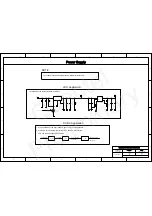
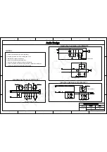
Charge golden capacitor or battery when VBAT is applied.
3. The width of VBAT trace is recommeded to be more than 2mm.
2. Module drains the maximum current around 1.6A in burst time (577us).
If unused, keep VRTC open.
1. VBAT ranges from 3.3V to 4.6V.
Reference Circuit of ADC
Close to the VBAT pins
Capacitance of C102 should
is recommended here.
be chosen by debugging to ensure
A 5.1V/1W zener diode
Module Design
As only powering the VRTC pin to keep the RTC will lead
an error for about 5 minutes a day, it is recommended
to power VBAT and VRTC pin at the same time when
RTC function is needed.
the max voltage drop during
the burst transmission
does not exceed 400mV.
The voltage range of ADC input channel is from 0 to 2.8V.
Please select a high-precision divider resistance.
4. Capacitance is arranged in ascending order, with the smallest one closing to the VBAT pins,
and all capacitance as close to the VBAT pins as possible.
A Pi match circuit is recommended to be added.
For RF layout, please refer to
RF_Layout_Application_Note.
Don't change those interface for other uses.
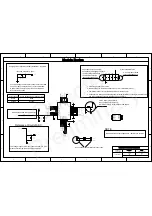
Active Antenna Power Supply Circuit
Active Antenna Power Supply Circuit
AntennaType
Active
Passive
Need
No need
MC60 module does not support PCM / BT/SD card function
NOTE
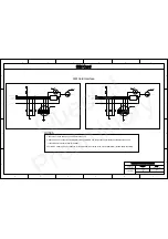
B101
XH414
+
C101
NM_Golden capacitor
R104
R106
C103
1uF
C105
33pF
+
C102
470uF
C106
10pF
D101
1
MICP
2
MICN
3
SPKP
4
SPKN
5
PWRKEY
6
ADC
7
SD_CMD
8
SD_CLK
9
SD_DATA
10
SIM2_CLK
11
SIM2_DATA
12
SIM2_RST
13
SIM2_VDD
14
GND
15
GNSS_ANT
16
SI
M
_
GND
17
RESERVED
18
SI
M
1
_VDD
19
SI
M
1
_CLK
20
SI
M
1
_RST
21
SI
M
1
_DATA
22
GNSS_TXD
23
GNSS_RXD
24
RXD_AUX
25
TXD_AUX
26
GNSS_VCC
27
GND
28
GNSS_VCC_EN
29
DBG_TXD
30
DBG_RXD
31
GND
32
BT_ANT
33
TXD
34
RXD
35
RI
36
DCD
37
DTR
38
CTS
39
RTS
40
GND
41
RF_ANT
42
GND
43
VDD_EXT
44
GND
45
GND
46
RESERVED
47
NETLI
G
HT
48
GND
49
GND
50
VBAT
51
VBAT
52
VRTC
53
LOUDSPKN
54
LOUDSPKP
U101-A
MC60
55
RESERVED
56
RESERVED
57
RESERVED
58
RESERVED
59
PCM_CLK
60
PCM_OUT
61
PCM_SYNC
62
PCM_IN
63
RESERVED
64
RESERVED
65
RESERVED
66
RESERVED
67
RESERVED
68
RESERVED
U101-B
MC60
C107
NM
C108
NM
R101
0R
J101
RF_ANT
C111
NM
C112
NM
R103
0R
J103
GNSS_ANT
C115
100nF
C104
100nF
R107
0R
R108
0R
R109
10R
L1
47nH
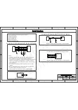
[1]
VRTC
[1]
ADC
VBAT
VOLTAGE_INPUT
[6]
DBG_RXD
[6]
DBG_TXD
[3]
MICP
[3]
MICN
[3]
SPKP
[3]
SPKN
[5,6]
PWRKEY
[1]
ADC
[4]
SIM2_CLK
[4] SIM2_DATA
[4]
SIM2_RST
[4]
SIM2_VDD
[4]
S
IM
1_
V
D
D
[4]
SI
M
1
_CLK
[4]
S
IM
1_
R
S
T
[4]
SI
M
1
_DATA
[2]
GNSS_VCC_EN
VCC_3V3
[3]
LOUDSPKP
[3]
LOUDSPKN
[1]
VRTC
VBAT
VDD_EXT
[1
]
G
NSS_TXD
[1]
GNSS_RXD
[5]
NETLI
G
HT
[6]
CTS
[6]
RTS
[1]
R
X
D
_
A
U
X
[1]
T
X
D
_
A
U
X
[6]
DTR
[6]
TXD
[6]
RXD
[6]
RI
[6]
DCD
[4]
S
IM
_
G
N
D
[1] GNSS_TXD
[1]
RXD_AUX
[1]
TXD_AUX
[1]
GNSS_RXD
[1,2,6]
VCC_3V3
Quectel
Preliminary


