background image

M20 Hardware Design                                                                                                                           


7.3.1 Board-to-board connector 

This section provides specifications for the 50-pin board-to-board connector which serves as 
physical interface to the host application. The receptacle assembled on the M20 module is type 
Hirose DF12C or DF12A. Mating headers from Hirose are available in different stacking heights. 

Table 38: Ordering information DF12 series 

Item 

Part number 

Stacking height

HRS number 

DF12A(3.0)-50DS-0.5V(81)

3.0 537-0634-7-81 

Receptacle on M20 

DF12C(3.0)-50DS-0.5V(81)

3.0 537-0694-9-81 

DF12E(3.0)-50DP-0.5V(81)

3.0 537-0834-6-** 

DF12E(3.5)-50DP-0.5V(81)

3.5 537-0534-2-** 

DF12E(4.0)-50DP-0.5V(81)

4.0 537-0559-3-** 

Headers DF12 series 

DF12E(5.0)-50DP-0.5V(81)

5.0 537-0584-0-** 


Note: Please contact Hirose for details on other types of mating headers. Asterixed HRS 

numbers denote different types of packaging. 

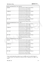
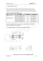
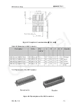
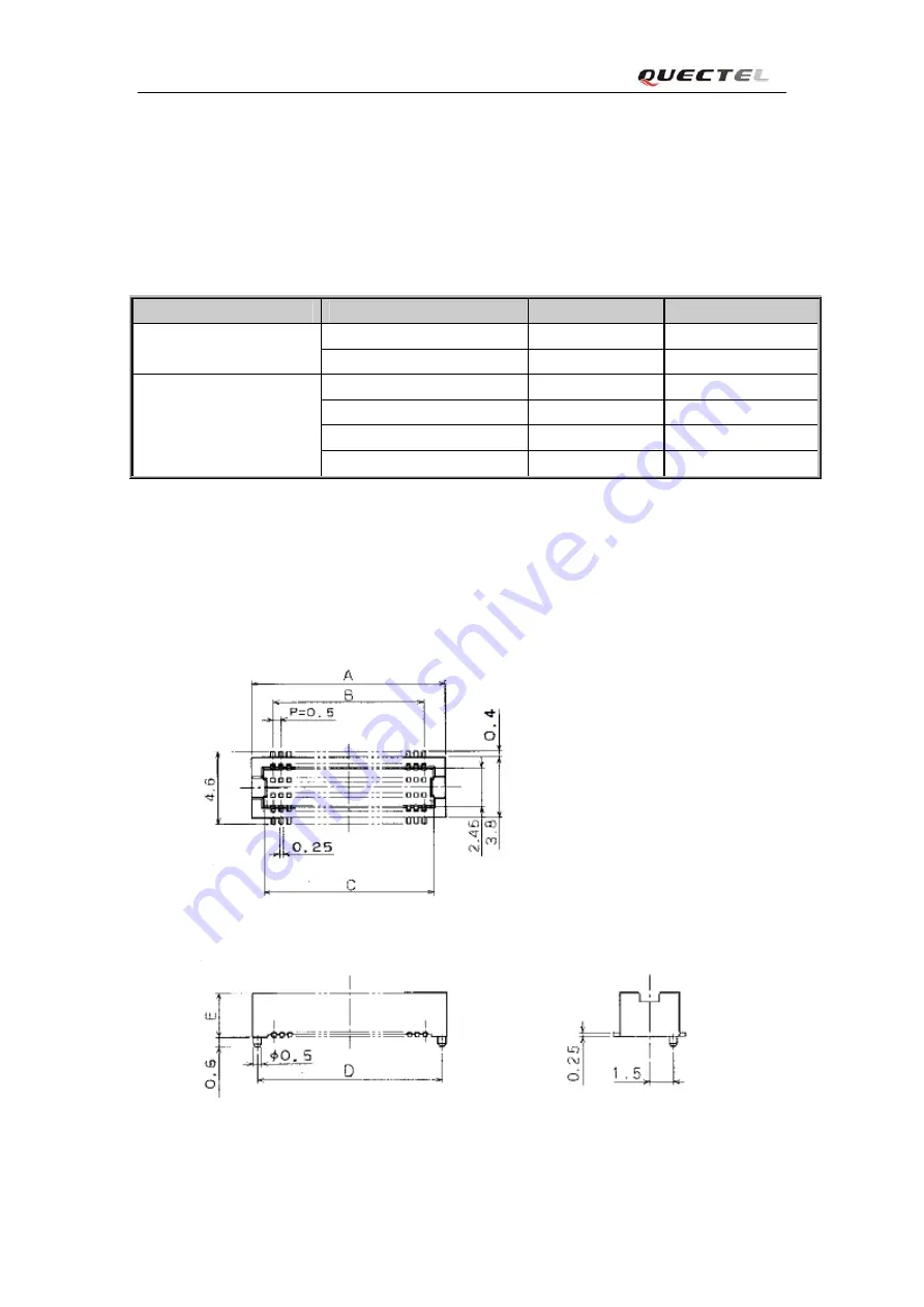
7.3.2 Mechanical dimensions of the DF12 header (without metal fitting) 


Figure 46: D

imensions


of


the


DF12


header

Unit:


mm


M20_HD_V1.01        


- 74 -   


Quectel
Summary of Contents for M20

Page 1: ...M20 Quectel Cellular Engine Hardware Design M20_HD_V1 01 ...

Page 2: ...validation of this product designed by Quectel within a larger electronic system remains the responsibility of the customer or the customer s system integrator All specifications supplied herein are subject to change Copyright This document contains proprietary technical information which is the property of Quectel Limited copying of this document and giving it to others and the using or communica...

Page 3: ...arging interface 33 3 5 1 Battery pack characteristics 34 3 5 2 Recommended battery pack 35 3 5 3 Implemented charging technique 36 3 5 4 Operating modes during charging 38 3 5 5 Charger requirements 39 3 6 Power saving 40 3 6 1 Minimum functionality mode 40 3 6 2 SLEEP mode 40 3 6 3 Wake up module from the SLEEP mode 41 3 7 Summary of state transition except SLEEP mode 41 3 8 RTC backup 41 3 9 Se...

Page 4: ...tures 66 5 4 Power supply ratings 66 5 5 Current consumption 67 5 6 Electro static discharge 70 6 Product information 71 7 Mechanical dimension 72 7 1 Mechanical dimensions of module 72 7 2 Footprint of recommendation 73 7 3 Mounting module in the host 73 7 3 1 Board to board connector 74 7 3 2 Mechanical dimensions of the DF12 header without metal fitting 74 7 3 3 Physical photo of the DF12 conne...

Page 5: ...CAL SPEAKER OUTPUT CHARACTERISTIC 54 TABLE 19 PIN DEFINITION OF THE DAI INTERFACE 54 TABLE 20 PIN DEFINITION OF THE SIM INTERFACE 55 TABLE 21 PIN DESCRIPTION AMPHENOL SIM CARD HOLDER 58 TABLE 22 PIN DESCRIPTION MOLEX SIM CARD HOLDER 58 TABLE 23 PIN DEFINITION OF THE ADC 59 TABLE 24 CHARACTERISTICS OF THE ADC 59 TABLE 25 BEHAVIOURS OF THE RI0 59 TABLE 26 WORKING STATE OF NETLIGHT 61 TABLE 27 PRODUC...

Page 6: ...M20 Hardware Design TABLE 41 GPRS MULTI SLOT CLASSES 80 M20_HD_V1 01 5 Quectel ...

Page 7: ...HARACTERISTIC 43 FIGURE 20 CONNECTION OF SERIAL INTERFACES 44 FIGURE 21 CONNECTION OF SOFTWARE UPGRADE 46 FIGURE 22 CONNECTION OF SOFTWARE DEBUGGING 47 FIGURE 23 RS 232 LEVEL CONVERTER CIRCUIT 47 FIGURE 24 ELECTRET MICROPHONE INTERFACE CONFIGURATION OF AIN1 49 FIGURE 25 ELECTRET MICROPHONE INTERFACE CONFIGURATION OF AIN2 50 FIGURE 26 SIGNAL SOURCE INTERFACE CONFIGURATION OF AIN1 AIN2 50 FIGURE 27 ...

Page 8: ...T MM 74 FIGURE 47 FOOTPRINT OF RECOMMENDATION UNIT MM 75 FIGURE 48 PHYSICAL PHOTOS OF THE DF12 CONNECTORS 75 FIGURE 49 PHYSICAL PHOTOS OF THE UF L R SMT CONNECTOR UNIT MM 76 FIGURE 50 MECHANICALS OF UF L LP CONNECTORS 77 FIGURE 51 SPACE FACTOR OF MATED CONNECTOR UNIT MM 77 FIGURE 52 TOP VIEW OF THE MODULE 78 FIGURE 53 BOTTOM VIEW OF THE MODULE 78 FIGURE 54 RADIO BLOCK STRUCTURE OF CS 1 CS 2 AND CS...

Page 9: ... Description of change 1 00 2009 09 8 Yong AN Initial 1 01 2009 09 17 Yong AN Add SIM_GND Pin name descriptions Modify Figure 33 and Figure 34 about SIM card circuit Add current consumption of 2 Rx and 3 Tx in data mode Modify ordering information content in Chapter 6 Quectel ...

Page 10: ...hase 2 AT command set for GSM Mobile Equipment ME 4 GSM 07 10 Support GSM 07 10 multiplexing protocol 5 GSM 07 05 Digital cellular telecommunications Phase 2 Use of Data Terminal Equipment Data Circuit terminating Equipment DTE DCE interface for Short Message Service SMS and Cell Broadcast Service CBS 6 GSM 11 14 Digital cellular telecommunications system Phase 2 Specification of the SIM Applicati...

Page 11: ...tal Signal Processor DTE Data Terminal Equipment typically computer terminal printer DTR Data Terminal Ready DTX Discontinuous Transmission EFR Enhanced Full Rate EGSM Enhanced GSM EMC Electromagnetic Compatibility ESD Electrostatic Discharge ETS European Telecommunication Standard FCC Federal Communications Commission U S FDMA Frequency Division Multiple Access FR Full Rate GMSK Gaussian Minimum ...

Page 12: ...ode USSD Unstructured Supplementary Service Data VSWR Voltage Standing Wave Ratio Vmax Maximum Voltage Value Vnorm Normal Voltage Value Vmin Minimum Voltage Value VIHmax Maximum Input High Level Voltage Value VIHmin Minimum Input High Level Voltage Value VILmax Maximum Input Low Level Voltage Value VILmin Minimum Input Low Level Voltage Value VImax Absolute Maximum Input Voltage Value VImin Absolu...

Page 13: ...ding an aircraft Make sure it being switched off The operation of wireless appliances in an aircraft is forbidden to prevent interference with communication systems Forget to think much of these instructions may lead to the flight safety or offend against local legal action or both Do not operate the cellular terminal or mobile in the presence of flammable gases or fumes Switch off the cellular te...

Page 14: ... calls In order to make or receive calls the cellular terminal or mobile must be switched on and in a service area with adequate cellular signal strength Some networks do not allow for emergency call if certain network services or phone features are in use e g lock functions fixed dialing etc You may have to deactivate those features before you can make an emergency call Also some networks require...

Page 15: ...p to easily develop customer s application z Two audio channels include two microphone inputs and two speaker outputs This can be easily configured by AT command The module is designed with power saving technique so that the current consumption is as low as 1 1mA in SLEEP mode when DRX is 5 The M20 is integrated with the Internet protocols extended Internet service AT commands are developed for cu...

Page 16: ... z Support Unstructured Supplementary Services Data USSD SMS z MT MO CB Text and PDU mode z SMS storage SIM card FAX Group 3 Class 1 SIM interface Support SIM card 1 8V 3V Antenna interface Connect via 50Ω antenna connector or antenna pad Audio feature Speech codec modes z Half Rate ETS 06 20 z Full Rate ETS 06 10 z Enhanced Full Rate ETS 06 50 06 60 06 80 z Adaptive Multi Rate AMR z Echo Cancella...

Page 17: ... error could increase Table 4 Coding schemes and maximum net data rates over air interface Coding scheme 1 Timeslot 2 Timeslots 4 Timeslots CS 1 9 05kbps 18 1kbps 36 2kbps CS 2 13 4kbps 26 8kbps 53 6kbps CS 3 15 6kbps 31 2kbps 62 4kbps CS 4 21 4kbps 42 8kbps 85 6kbps 2 2 Functional diagram The following figure shows a block diagram of the M20 module and illustrates the major functional part z The ...

Page 18: ...luation board In order to help customer on the application of M20 Quectel can supply an Evaluation Board EVB that hosts the module directly with appropriate power supply SIM card holder RS 232 serial interface handset RJ11 port earphone port antenna and other peripherals to control or test the module For details please refer to the M20_EVB_UGD document M20_HD_V1 01 17 Quectel ...

Page 19: ...CRIPTION DC CHARACTERISTICS COMMENT VBAT I VBAT pins of the B2B are dedicated to connect the supply voltage The power supply of module has to be a single voltage source of VBAT 3 4V 4 5V It must be able to provide sufficient current in a transmitting burst which typically rises to 2A Mostly these 5 pins are voltage inputs Vmax 4 5V Vmin 3 4V Vnorm 4 0V VCHG I Voltage input for the charging circuit...

Page 20: ...ng this key for a moment when turn on or turn off the module VILmax 0 3 VBAT VIHmin 0 7 VBAT VImax VBAT Pull up to VBAT internally Emergency shutdown PIN NAME I O DESCRIPTION DC CHARACTERISTICS COMMENT EMERG_OF F I Voltage input for emergency shutdown under emergent situation EMERG_OFF should be pulled down for at least 20ms to shutdown the system in emergency The module can restart by PWRKEY oper...

Page 21: ... VILmax 0 67V VIHmin 1 7V VIHmax VDD_EXT 0 3 VOLmin GND VOLmax 0 34V VOHmin 2 0V VOHmax VDD_EXT If unused keep this open DAI interface PIN NAME I O DESCRIPTION DC CHARACTERISTICS COMMENT RXDDAI I Receive digital audio data TFSDAI O Frame synchronization SCLK O Serial bit clock TXDDAI O Transmit digital audio data VILmin 0V VILmax 0 67V VIHmin 1 7V VIHmax VDD_EXT 0 3 VOLmin GND VOLmax 0 34V VOHmin ...

Page 22: ...nterface PIN NAME I O DESCRIPTION DC CHARACTERISTICS COMMENT SIM_VDD O Voltage supply for SIM card The voltage can be selected by software automatically 1 8V or 3V SIM_DATA I O SIM data SIM_CLK O SIM clock SIM_RST O SIM reset VIHmin 0 7 SIM_VDD VOHmin 0 8 SIM_VDD VOLmax 0 4V When SIM_VDD 3V VILmax 0 4V When SIM_VDD 1 8V VILmax 0 2 SIM_VDD VOHmin 0 9 SIM_VDD When SIM_VDD 3V VOLmax 0 4V When SIM_VDD...

Page 23: ...he module will automatically enter SLEEP mode if DTR is set to high level when the slow clocking mode is enabled by setting AT QSCLK 1 and there is no other task under execution In this case the current consumption of module will be reduced to very low level During SLEEP mode the module can still receive paging message for voice or SMS from GSM system GSM IDLE Software is active and the main contr...

Page 24: ...ll accessible If the slow clocking mode is enabled by AT QSCLK 1 the power consumption would be less than 0 9mA Alarm mode RTC alert function wakes up the module from POWER DOWN mode The module doesn t attempt to register to GSM network and only part of AT commands can be available The module would return to POWER DOWN mode if failing to issuing AT CFUN 1 within 90 seconds after wakeup Use the pin...

Page 25: ... voltage difference between the input source and the desired output VBAT a switching converter power supply would be preferable for its better efficiency especially with the 2A peak current in burst mode of the module Figure 3 Reference circuit of the source power supply input When the power supply for the module can t provide current of 2A proper bigger capacitor is required so as to supply for t...

Page 26: ... talking mode Figure 4 shows the VBAT voltage drop and current ripple at the maximum power transmitting phase the test condition is VBAT 4 0V VBAT voltage source maximum output current 2A C1 100µF tantalum capacitor ESR 0 7Ω and C2 1µF Max 400mV Burst 1 6A 4 615ms 577us IBAT VBAT Figure 4 Ripple in supply voltage during transmitting burst 3 3 1 Power supply pins The VBAT pins are dedicated to conn...

Page 27: ... are described in following chapters z Via PWRKEY pin start normal operating mode please refer to chapter 3 4 1 1 z Via RTC interrupt start ALARM mode please refer to chapter 3 4 1 2 Note AT command can be sent to the module after it is powered on and Unsolicited Result Code RDY is received from the serial port0 However if the module was set to autobauding mode the URC RDY wouldn t be received fro...

Page 28: ... button directly A TVS component is indispensable to be placed nearby the button for ESD protection When pressing the key electrostatic strike may generate from finger A reference circuit is showed in Figure 6 S1 PWRKEY TVS1 Close to S1 Figure 6 Turn on the module by using button The power on scenario illustrates as in Figure 7 M20_HD_V1 01 27 Quectel ...

Page 29: ...ff state In alarm mode the module will not register to GSM network and the GSM protocol stack software is closed Thus the part of AT commands related with SIM card and the protocol stack will not be accessible and the others can be used Use the AT QALARM command to set the alarm time The RTC remains the alarm time if the module is powered off by AT QPOWD 1 or by PWRKEY pin Once the alarm time is e...

Page 30: ...edure Turn off module using the PWRKEY pin z Normal power down procedure Turn off module using command AT QPOWD z Over voltage or under voltage automatic shutdown Take effect when over voltage or under voltage is detected z Emergent power down procedure Turn off module using the EMERG_OFF pin 3 4 2 1 Turn off module using the PWRKEY pin Power down Customer s application can turn off the module by ...

Page 31: ... below NORMAL POWER DOWN After this moment no further AT command can be executed And then the module enters the POWER DOWN mode only the RTC is still active The POWER DOWN mode can also be indicated by VDD_EXT pin which is a low level voltage in this mode Please refer to document 1 for detail about the AT command of AT QPOWD 3 4 2 3 Over voltage or under voltage automatic shutdown The module will ...

Page 32: ...utdown The module can be shut down by driving the pin EMERG_OFF to a low level voltage for over 20ms and then releasing it The EMERG_OFF line can be driven by an Open Drain Collector driver or a button The circuit illustrates as the following figures 4 7K 47K Emergency shutdown impulse EMERG_OFF Figure 9 Reference circuit for EMERG_OFF by using driving circuit S1 EMERG_OFF TVS1 Close to S1 Figure ...

Page 33: ... the module by driving the PWRKEY to a low level voltage for certain time which is similar to the way to turn on module Before restarting the module at least 500ms should be delayed after detecting the low level of VDD_EXT The restart scenario illustrates as the following figure VDD_EXT OUTPUT H PWRKEY INPUT VIL 0 3 VDD_EXT Delay 500ms Turn off Pull down the PWRKEY to turn on the module Restart Fi...

Page 34: ...ource is used to charging the battery In this case when the battery is charged full the charging circuit will stop working but the charging function would be re activated when the battery voltage drops to certain level The battery is either in discharging mode or in charging mode which could significantly shorten its life cycle Therefore it should always be cautious to use the internal charging fu...

Page 35: ...l power supply is present Q1 is cut off and the module is powered by external supply Otherwise Q1 is turned on and the module is supplied by the battery The Q1 P channel MOSFET must be able to supply continuous drain current bigger than 2A Moreover on resistance of Drain to Source should be as small as possible which means lower thermal power dissipation and voltage drop U2 is a charging IC which ...

Page 36: ...nternal resistance of the battery and the protection circuit should be as low as possible It is recommended that the battery internal resistance should not exceed 70mΩ and the internal resistance include battery and protection circuit of battery pack should not exceed 130mΩ z The battery pack must be protected from reverse pole connection z The Li Ion Polymer battery charging protection parameter ...

Page 37: ...VCHG pin and connect the battery to the VBAT pin When the module detects the charger supply and the battery are both present battery charging happens If there is no charger supply or no battery present the charging function would not be enabled Normally there are three main states in whole charging procedure z DDLO charging and UVLO charging z CC constant current charging or fast charging z CV con...

Page 38: ...er CC charging ending the module automatically enters constant voltage charging When charging current steadily decreases to 50mA the module begins to carry out 30 minutes charging delay The CV charging will terminate after this delay Charging hold only for Li Ion battery The charging hold state is exclusively for Li Ion battery When the charger is applied a voice call is connected and the battery ...

Page 39: ... in various working modes such as SLEEP TALK and GPRS DATA It is named as Charging mode When a charger is connected to the module s VCHG pin the battery is connected to the VBAT pin and the module is in POWER DOWN mode the module enters the GHOST mode Off and charging The following table gives the differences between Charging mode and GHOST mode M20_HD_V1 01 38 Quectel ...

Page 40: ...T mode AT commands listed in Table 12 can be used For further instruction refer to document 1 Table 12 AT Commands available in the GHOST mode AT command Function AT QALARM Set alarm time AT CCLK Set data and time of RTC AT QPOWD Power down the module AT CBC Indicated charging state and voltage AT CFUN Start or close the protocol Setting AT command AT CFUN 1 to the module will transfer it from GHO...

Page 41: ...ccessible but all AT commands correlative with RF function or SIM card function will not be accessible If the module has been set by AT CFUN 4 the RF function will be closed the serial port is still active In this case all AT commands correlative with RF function will not be accessible After the module is set by AT CFUN 0 or AT CFUN 4 it can return to full functionality by AT CFUN 1 For detailed i...

Page 42: ...on except SLEEP mode Table 13 Summary of state transition Further mode Current mode POWER DOWN Normal mode Alarm mode POWER DOWN Use PWRKEY Turn on the module by RTC alarm Normal mode AT QPOWD use PWRKEY pin or use EMERG_OFF pin Set alarm by AT QALARM and then turn off the module When the timer expires the module turns on automatically and enters Alarm mode Alarm mode Use PWRKEY pin or wait module...

Page 43: ...hargeable battery RTC Core 3 9K Module VRTC Rechargeable Backup Battery Figure 17 RTC supply from rechargeable battery RTC Core 3 9K Module VRTC Large capacitance Capacitor Figure 18 RTC supply from capacitor Coin type rechargeable capacitor such as XH414H IV01E form Seiko can be used M20_HD_V1 01 42 Quectel ...

Page 44: ...rovides two unbalanced asynchronous serial ports serial port0 and serial port1 The module is designed as a DCE Data Communication Equipment following the traditional DCE DTE Data Terminal Equipment connection The module and DTE are connected through the following signal in Figure 20 M20_HD_V1 01 43 Quectel ...

Page 45: ...ule supports hardware flow control in default When the module is used as a modem DCD0 and RI0 should be connected Furthermore RI0 could indicate the host controller when an event happens such as an incoming voice call a URC data export Serial Port 1 z TXD1 Send data to the RXD signal line of DTE z RXD1 Receive data from the TXD signal line of DTE Note Serial port 1 can also support hardware flow c...

Page 46: ...ata CSD FAX etc Multiplexing function is supported at Serial Port 0 So far only the basic mode of multiplexing is available z Support the communication baud rates as the following 75 150 300 600 1200 2400 4800 9600 14400 19200 28800 38400 57600 115200 Default setting is 115200bps z Support the following baud rates for Autobauding function 4800 9600 19200 38400 57600 115200bps After setting a fixed...

Page 47: ...ot be detected before inputting AT character Serial Port 1 z Two data lines TXD1 and RXD1 z Two hardware flow control lines RTS1 and CTS1 z Serial port 1 is used for software debugging It cannot be used for AT command GPRS service CSD call and FAX call It doesn t support multiplexing and autobauding function 3 9 2 Software upgrade and software debug The TXD0 RXD0 can be used to upgrade software wh...

Page 48: ...evel shifter circuit when the module is connected to a PC 9 8 7 6 5 4 3 2 1 15 14 8 9 11 12 5 7 6 10 4 26 2 27 13 18 20 21 16 17 19 22 23 24 3 1 25 28 GND TO PC serial port SP3238 3V GND GND T5OUT SHUTDOWN V GND V VCC T4OUT T2OUT T3OUT T1OUT R3IN R2IN R1IN STATUS 3V ONLINE R1OUT R2OUT R3OUT R1OUT GND T5IN T4IN T3IN T2IN T1IN C2 C2 C1 C1 RXD DTR RTS RI CTS TXD DCD Module Figure 23 RS 232 level conv...

Page 49: ... of receiver and speaker AT QECHO is to set the parameters for echo cancellation control AT QSIDET is to set the side tone gain level For more details please refer to document 1 Note z Use AT command AT QAUDCH to select audio channel 0 AIN1 AOUT1 normal audio channel the default value is 0 1 AIN2 AOUT2 aux_audio channel Table 16 Pin definition of audio interface Interface Name Pin Function MIC1P 4...

Page 50: ...IC should use AGND of the module as its ground instead of GND of the module to suppress TDD noise Electret Microphone 10pF 33pF 33pF 33pF Close to Microphone MIC1P MIC1N GND GND Difference layout Module GND GND 10pF 10pF GND GND ESD ANTI ESD ANTI AGND 1K AGND VMIC_2V8 1K 1 5K 1 5K 10uF Figure 24 Electret microphone interface configuration of AIN1 AIN2 channel comes with an internal bias supply for...

Page 51: ... AIN2 channels are connected to other type of audio signal source instead of electret microphone for example an op amp or a moving coil type microphone it is recommended to insert two 10μF capacitors for decoupling 10pF 33pF 33pF 33pF Close to Microphone MICxP MICxN GND Differential layout Module GND 10pF GND GND ESD ANTI ESD ANTI AGND 10µF 10µF Signal source Figure 26 Signal source interface conf...

Page 52: ...pF Close to speaker GND GND 10pF ESD ANTI ESD ANTI Moudule Figure 27 Speaker interface configuration of AOUT1 SPK1P SPK1N Differential layout Amplifier circuit 10pF 10pF 33pF 33pF 33pF Close to speaker GND GND 10pF ESD ANTI ESD ANTI Module Figure 28 Speaker interface with amplifier in AOUT1 M20_HD_V1 01 51 Quectel ...

Page 53: ...er interface configuration of AOUT2 SPK2P AGND Differential layout Amplifier circuit 10pF 10pF 33pF 33pF Close to speaker GND GND ESD ANTI ESD ANTI Module C2 C1 Figure 30 Speaker interface with amplifier in AOUT2 Note The value of C1 and C2 depends on the input impedance of audio amplifier M20_HD_V1 01 52 Quectel ...

Page 54: ...iguration Note The module supports optionally earphone detection and hook off in hardware In other words it is not supported in default hardware configuration If customer needs earphone detection or hook off detection please contact Quectel Table 17 Typical electret microphone input characteristic Parameter Min Typ Max Unit Working Voltage 1 2 1 5 2 0 V Working Current 200 500 μA External Micropho...

Page 55: ...aster mode Each pin definition of the DAI interface is listed in Table 19 Table 19 Pin definition of the DAI interface Interface Name Pin Function RXDDAI 7 Receive digital audio signal TFSDAI 8 Frame synchronization signal SCLK 9 Serial bit clock DAI TXDDAI 10 Transmit digital audio signal The SLCK clock signal is an output generating a 256KHz bit clock as master The TFSDAI frame sync signal is an...

Page 56: ... specification for FAST 64 kbps SIM card which is intended for use with a SIM application Tool kit Both 1 8V and 3 0V SIM cards are supported The SIM interface is powered from an internal regulator in the module Table 20 Pin definition of the SIM interface Name Pin Function SIM_VDD 2 Supply power for SIM Card Automatic detection of SIM card voltage 3 0V 10 and 1 8V 10 Maximum supply current is aro...

Page 57: ... VDD_EXT Module SMF05C SIM_VDD SIM_CLK SIM_DATA SIM_RST SIM_PRESENCE VCC GND RST VPP CLK I O 22R 22R 22R 1uF MOLEX 91228 SIM CARD GND 100K BB GPIO SIM_GND Figure 33 Reference circuit of using 8 pin SIM card socket In Figure 33 the pin SIM_PRESENCE is used to detect whether the tray of the Molex SIM socket which is used for holding SIM card is present in the card socket When the tray is inserted in...

Page 58: ... CARD GND SIM_GND Figure 34 Reference circuit of using 6 pin SIM card socket 3 11 2 Design considerations for SIM card holder For 6 pin SIM card holder it is recommended to use Amphenol C707 10M006 512 2 Please visit http www amphenol com for more information Figure 35 Amphenol C707 10M006 512 2 SIM card holder M20_HD_V1 01 57 Quectel ...

Page 59: ...round VPP C6 Not connect SIM_DATA C7 SIM Card data I O For 8 pin SIM card holder it is recommended to use Molex 91228 Please visit http www molex com for more information Figure 36 Molex 91228 SIM card holder Table 22 Pin description Molex SIM card holder Name Pin Function SIM_VDD C1 SIM Card Power supply SIM_RST C2 SIM Card Reset SIM_CLK C3 SIM Card Clock M20_HD_V1 01 58 Quectel ...

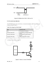
Page 60: ...y 2 7 mV 3 13 Behavior of the pin RI0 Table 25 Behaviours of the RI0 State RI respond Standby HIGH Voice calling Change to LOW then 1 Change to HIGH when call is established 2 Use ATH to hang up the call change to HIGH 3 Calling part hangs up change to HIGH 4 Change to HIGH when SMS is received Data calling Change to LOW then 1 Change to HIGH when data connection is established 2 Use ATH to hang u...

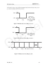
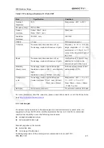
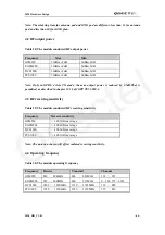
Page 61: ...g Off hook by ATA On hook by ATH Calling party on hook SMS received HIGH LOW Figure 37 RI0 behaviour of voice calling as a receiver RI0 Idle Ring Enter GPRS Ready Mode On hook by ATH HIGH LOW Figure 38 RI0 behaviour of data calling as a receiver RI0 Idle Calling On hook Talking HIGH LOW SMS received Idle Figure 39 RI0 behaviour of data calling as a caller M20_HD_V1 01 60 Quectel ...

Page 62: ...g state of this pin is listed in Table 26 Table 26 Working state of NETLIGHT State Module function Off The module is not running 64ms On 800ms Off The module is not synchronized with network 64ms On 2000ms Off The module is synchronized with network 64ms On 600ms Off GPRS data transfer is ongoing A reference circuit is shown in Figure 41 Module 300R 4 7K 47K VBAT NETLIGHT Figure 41 Reference circu...

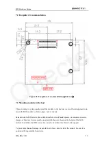
Page 63: ...d vice versa The antenna PAD and RF connector are shown in Figure 42 Figure 42 Antenna PAD and RF connector To minimize the loss on the RF cable RF cable should be chosen very carefully It is recommended that the insertion loss should try to meet the following requirements z GSM850 GSM900 1dB z DCS1800 PCS1900 1 5dB 4 1 Antenna installation 4 1 1 Antenna connector The module adopts Hirose s U FL R...

Page 64: ...ance 10MΩ min humidity high Insulation resistance 500MΩ min dry 96 hours at temperature of 40 and humidity of 95 Temperature cycle No damage cracks or parts dislocation Contact resistance 25mΩ max Center 15mΩ max Outer Temperature 40 5 to 35 90 5 to 35 Time 30min 3min 30min 3min 5 cycles Salt spray No excessive corrosion 5 salt water solution 48 hours For more information about the connector pleas...

Page 65: ... 5dB That is permitted as described in chapter 13 16 of 3GPP TS 51 010 1 4 3 RF receiving sensitivity Table 29 The module conducted RF receiving sensitivity Frequency Receive sensitivity GSM850 108 7dBm average EGSM900 108 5dBm average DCS1800 108 5dBm average PCS1900 108 1dBm average Note The antenna chosen will affect radiated receiving sensitivity 4 4 Operating frequency Table 30 The module ope...

Page 66: ...IC2N I 6 SIM_GND 45 MIC2P I 7 RXDDAI I O 44 MIC1P I 8 TFSDAI O 43 MIC1N I 9 SCLK O 42 AGND 10 TXDDAI O 41 PWRKEY I 11 Reserve O 40 EMERG_OFF I 12 ADC1 I 39 DCD0 O 13 NETLIGHT I O 38 CTS1 O 14 TXD1 O 37 CTS0 O 15 TXD0 O 36 RTS1 I 16 RXD1 I 35 DTR0 I 17 RXD0 I 34 RTS0 I 18 VRTC I O 33 Reserve 19 VCHG I 32 RI0 O 20 Reserve 31 VDD_EXT O 21 GND 30 VBAT I 22 GND 29 VBAT I 23 GND 28 VBAT I 24 GND 27 VBAT...

Page 67: ...rature is listed in the following table Table 33 Operating temperature Parameter Min Typ Max Unit Normal temperature 35 25 80 Restricted operation 45 to 35 80 to 85 Storage temperature 45 90 When the module works in this temperature range the deviations from the GSM specification may occur For example the frequency error or the phase error could increase 5 4 Power supply ratings Table 34 The modul...

Page 68: ... DATA mode GPRS 3 Rx 2Tx GSM850 EGSM 9001 DCS1800 PCS19002 430 410 290 320 mA DATA mode GPRS 2Rx 3Tx GSM850 EGSM 9001 DCS1800 PCS19002 560 530 350 400 mA DATA mode GPRS 4 Rx 1Tx GSM850 EGSM 9001 DCS1800 PCS19002 270 255 200 215 mA IVBAT Average supply current DATA mode GPRS 1 Rx 4Tx GSM850 EGSM 9001 DCS1800 PCS19002 510 530 360 405 mA Peak supply current during transmission slot Power control leve...

Page 69: ... Typical 125mA power level 19 Typical 90mA EGSM 900 power level 5 350mA Typical 230mA power level 12 Typical 120mA power level 19 Typical 90mA DCS 1800 power level 0 300mA Typical 170mA power level 7 Typical 110mA power level 15 Typical 90mA PCS 1900 power level 0 300mA Typical 185mA power level 7 Typical 110mA power level 15 Typical 90mA DATA mode GPRS 3 Rx 2 Tx CLASS 12 GSM850 power level 5 550m...

Page 70: ...vel 19 Typical 110mA DCS 1800 power level 0 300mA Typical 200mA power level 7 Typical 130mA power level 15 Typical 105mA PCS 1900 power level 0 300mA Typical 215mA power level 7 Typical 135mA power level 15 Typical 110mA DATA mode GPRS 1 Rx 4 Tx CLASS 12 GSM850 power level 5 660mA Typical 510mA power level 12 Typical 300mA power level 19 Typical 180mA EGSM 900 power level 5 660mA Typical 530mA pow...

Page 71: ...Proper ESD handing and packaging procedures must be applied throughout the processing handing and operation of any application using the module The measured values of module are shown as the following table Table 36 The ESD endurance Temperature 25 Humidity 45 Part Contact discharge Air discharge VBAT GND 5KV 10KV PWRKEY 4KV 8KV Antenna port 5KV 10KV SPK1P 1N SPK2P 2N MIC1P 1N MIC2P 2N 4KV 8KV Que...

Page 72: ...M20 Hardware Design 6 Product information Table 37 Ordering information Description Part Number Frequency Band RF Function M20 Q1 M20TM GSM850 EGSM900 DCS1800 PCS1900 GSM GPRS M20_HD_V1 01 71 Quectel ...

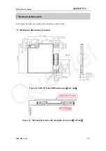
Page 73: ...ension This chapter describes the mechanical dimensions of the module 7 1 Mechanical dimensions of module Figure 43 M20 TOP and SIDE dimensions Unit mm Figure 44 M20 module matchs with the application board Unit mm M20_HD_V1 01 72 Quectel ...

Page 74: ... a frame plate rack or chassis Fasteners can be M20 screws plus suitable washers circuit board spacers or customized screws clamps or brackets Screws must be inserted with the screw head on the bottom of the M20 module In addition the B2B connection can also be utilized to achieve better support To prevent mechanical damage be careful not to force bend or twist the module Be sure it is positioned ...

Page 75: ...art number Stacking height HRS number DF12A 3 0 50DS 0 5V 81 3 0 537 0634 7 81 Receptacle on M20 DF12C 3 0 50DS 0 5V 81 3 0 537 0694 9 81 DF12E 3 0 50DP 0 5V 81 3 0 537 0834 6 DF12E 3 5 50DP 0 5V 81 3 5 537 0534 2 DF12E 4 0 50DP 0 5V 81 4 0 537 0559 3 Headers DF12 series DF12E 5 0 50DP 0 5V 81 5 0 537 0584 0 Note Please contact Hirose for details on other types of mating headers Asterixed HRS numb...

Page 76: ...5V 81 537 0834 6 81 50 14 7 12 0 13 2 2 3 DF12E 3 5 50DP 0 5V 81 537 0534 2 81 50 14 7 12 0 13 2 2 8 DF12E 4 0 50DP 0 5V 81 537 0559 3 81 50 14 7 12 0 13 2 3 3 DF12E 5 0 50DP 0 5V 81 537 0584 0 81 50 14 7 12 0 13 2 4 3 Without metal fitting Without boss 7 3 3 Physical photo of the DF12 connector Figure 48 Physical photos of the DF12 connectors M20_HD_V1 01 75 Quectel ...

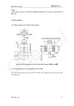
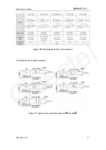
Page 77: ...B side 7 4 RF connector 7 4 1 Physical photo of the UF L R SMT connector Figure 49 Physical photos of the UF L R SMT connector Unit mm 7 4 2 Matching connector on the application side of M20 Five types of female connector can match UF L R SMT The mechanicals of them are listed in the following figure M20_HD_V1 01 76 Quectel ...

Page 78: ...M20 Hardware Design Figure 50 Mechanicals of UF L LP connectors 7 4 3 Space factor of mated connector Figure 51 Space factor of mated connector Unit mm M20_HD_V1 01 77 Quectel ...

Page 79: ...M20 Hardware Design 7 5 Top view of the module Figure 52 Top view of the module 7 6 Bottom view of the module Figure 53 Bottom view of the module M20_HD_V1 01 78 Quectel ...

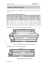
Page 80: ...ta rate Kb s CS 1 1 2 3 3 181 40 4 456 0 9 05 CS 2 2 3 3 6 268 16 4 588 132 13 4 CS 3 3 4 3 6 312 16 4 676 220 15 6 CS 4 1 3 12 428 16 456 21 4 Radio block structure of CS 1 CS 2 and CS 3 is shown as Figure 54 rate 1 2 convolutional coding puncturing 456 bits USF BCS Radio Block Figure 54 Radio block structure of CS 1 CS 2 and CS 3 Radio block structure of CS 4 is shown as Figure 55 block code no ...

Page 81: ...uplink timeslots The active slots determine the total number of slots the GPRS device can use simultaneously for both uplink and downlink communications The description of different multi slot classes is shown in Table 41 Table 41 GPRS multi slot classes Multislot class Downlink slots Uplink slots Active slots 1 1 1 2 2 2 1 3 3 2 2 3 4 3 1 4 5 2 2 4 6 3 2 4 7 3 3 4 8 4 1 5 9 3 2 5 10 4 2 5 11 4 3 ...

Page 82: ...M20 Hardware Design M20_HD_V1 01 81 Shanghai Quectel Wireless Solutions Co Ltd Room 801 Building E No 1618 Yishan Road Shanghai China 201103 Tel 86 21 5108 2965 Mail info quectel com ...

Reviews:

Related manuals for M20