


LTE Standard Module Series
EG25-GL_Hardware_Design 49 / 96
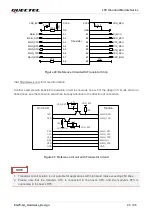
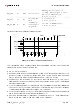
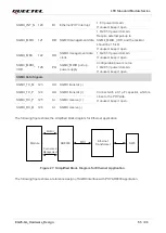
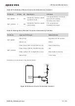
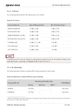
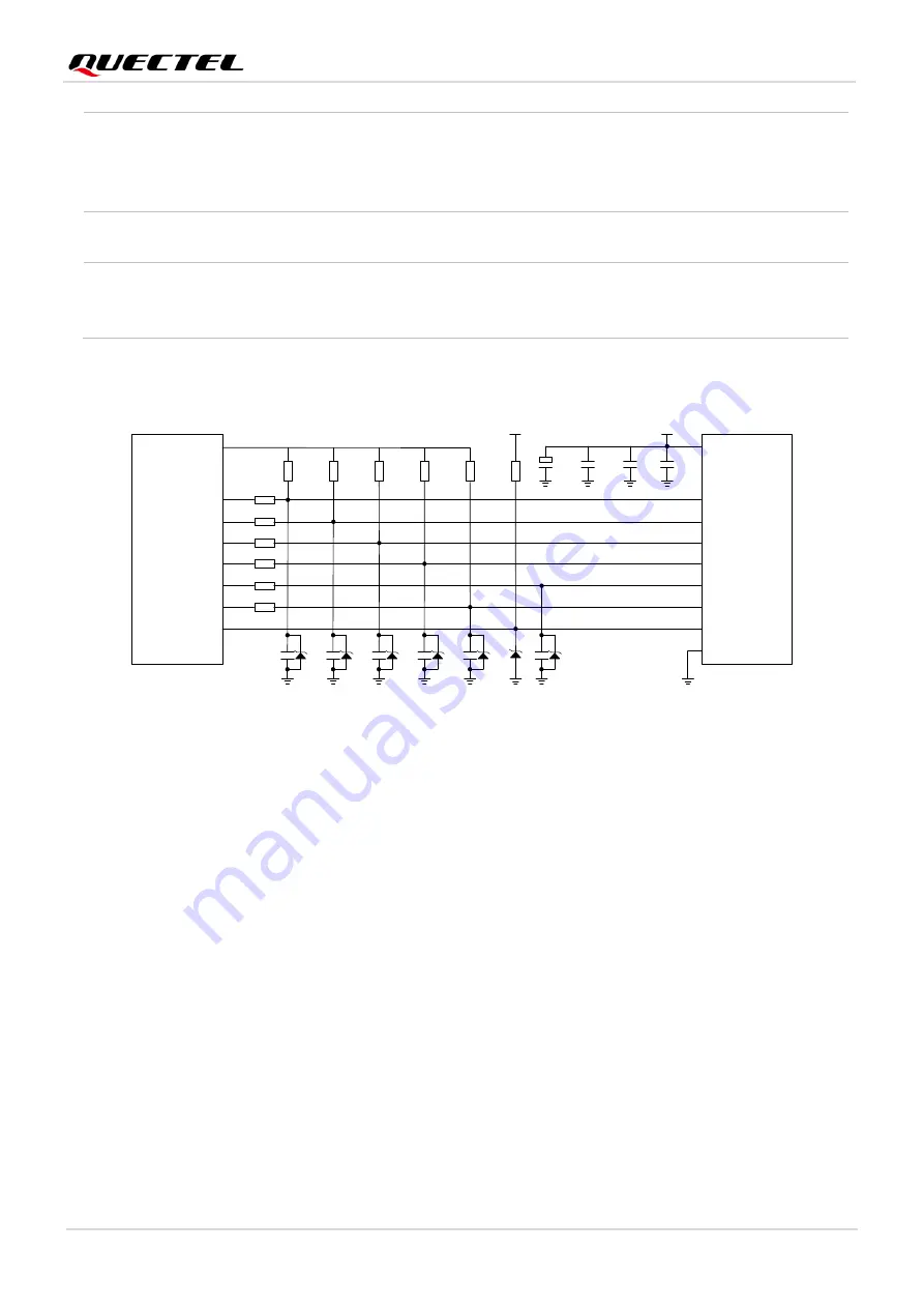
The following figure shows a reference design of SD card.
SD Card Connector
DAT2
CD/DAT3
CMD
VDD
CLK
VSS
DAT0
DAT1
DETECTIVE
Module
SD_DATA3
SD_DATA2
SD_DATA1
SD_PU_VDD
SD_DATA0
SD_CLK
SD_CMD
SD_DET
R1 0R
R7
NM
R8
NM
R9
NM
R10
NM
R11
NM
R12
470K
VDD_EXT
VDD_3V
R2 0R
R3 0R
R4 0R
R5 0R
R6 0R
C2
NM
D2 C3
NM
D3 C4
NM
D4 C5
NM
D5
C6
NM
D6
C1
NM
D1
D7
+
C10
100
μ
F
C9
100 nF
C8
33 pF
C7
10 pF
Figure 25: Reference Circuit of SD Card Interface
In SD card interface design, in order to ensure good communication performance with SD card, the
following design principles should be complied with:
⚫
SD_DET must be connected.
⚫
The voltage range of SD card power supply VDD_3V is 2.7
–3.6 V and a sufficient current up to 0.8 A
should be provided. As the maximum output current of SD_PU_VDD is 50 mA which can only be
used for SDIO pull-up resistors, an externally power supply is needed for SD card.
⚫
To avoid jitter of bus, resistors R7
–R11 are needed to pull up the SDIO to SD_PU_VDD. Value of
these resistors is among 10
–100 kΩ and the recommended value is 100 kΩ. SD_PU_VDD should be
used as the pull-up power.
⚫
In order to adjust signal quality, it is recommended to add 0
Ω resistors R1–R6 in series between the
module and the SD card. The bypass capacitors C1
–C6 are reserved and not mounted by default. All
resistors and bypass capacitors should be placed close to the module.
⚫
In order to offer good ESD protection, it is recommended to add a TVS diode on SD card pins near
the SD card connector with junction capacitance less than 15 pF.
⚫
Keep SDIO signals far away from other sensitive circuits/signals such as RF circuits, analog signals,
etc., as well as noisy signals such as clock signals, DC-DC signals, etc.
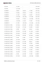
SD_CMD
33
DIO
SD card command
SDIO signal level can be selected
according to SD card supported level, see
SD 3.0 protocol for more details.
If unused, keep it open.
SD_DET
23
DI
SD card insertion
detect
1.8 V power domain.
If unused, keep it open.
SD_PU_VDD
34
PO
1.8/2.85 V output
power for SD card
pull-up circuits
Cannot be used for SD card power.
If unused, keep it open.