background image

                                                                                                      5G  Module  Series


5G-M2_EVB_User_Guide                                                                                                                            16  / 34 


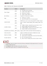
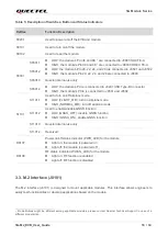
Table 5: Description of Switches, Button and Status Indicators 


3.3. M.2 Interface (J0101) 


The M.2 interface  (J0101) is designed to mount applicable modules. This interface allows  engineers to 

easily test functionalities or develop applications based on the module. 


1

  Pin  definitions  might  be  different  among  applicable  modules,  please  contact  Quectel  Technical  Support  in  case  of  a 

different pin definition. 

RefDes 

Function Description 

S0201 

Used to power on/off the EVB and module 

S0101 

Used to turn on/off the module 

S0102 

Used to reset the module 

S0301 

S0301.1 


LOW: 

the module’s Pin 38 and 68

  1

  are connected to J0803 SLIC TE-A 


HIGH: 

the module’s Pin 38 and 68

 1

 are connected to J0803 CODEC TE-A 

S0301.2 


LOW: 

the module’s Pin 20, 22, 24, and 28 are connected to J0501 and J0502 


HIGH: the modul

e’s Pin 20, 22, 24, and 28 are connected to J0803 

S0301.3 

Quectel internal use only 

S0301.4 


LOW: 

the module’s PCIe is connected to J0401 USB Type-B Connector 


HIGH: 

the module’s PCIe is connected to J0501 and J0502 

S1101 

S1101.1 

Used to turn on/off airplane mode 


LOW (FLIGHT_MD): turn on airplane mode 


HIGH (NORMAL_MD): turn off airplane mode 

S1101.2 

Used to enable/disable GNSS function 


LOW (GNSS_OFF): disable GNSS function 


HIGH (GNSS_ON): enable GNSS function 

S1101.3 

Quectel internal use only 

S1101.4 

Reserved 

D0107 

Power on/off status indicator (PWR_LED) for the module 


Light on: the module is powered on 


Light off: the module is powered off 

D0108 

RF status indicator (WWAN_LED) for the module 


Light on: RF function is enabled 


Light off: RF function is disabled 
Summary of Contents for 5G-M2 EVB

Page 1: ...5G M2 EVB User Guide 5G Module Series Version 1 0 Date 2021 11 18 Status Released ...

Page 2: ...loy commercially reasonable efforts to provide the best possible experience you hereby acknowledge and agree that this document and related services hereunder are provided to you on an as available basis We may revise or restate this document from time to time at our sole discretion without any prior notice to you Use and Disclosure Restrictions License Agreements Documents and information provide...

Page 3: ...plement module functionality certain device data are uploaded to Quectel s or third party s servers including carriers chipset suppliers or customer designated servers Quectel strictly abiding by the relevant laws and regulations shall retain use disclose or otherwise process relevant data for the purpose of performing the service only or as permitted by applicable laws Before data interaction wit...

Page 4: ...ference on sensitive medical equipment so please be aware of the restrictions on the use of wireless devices when in hospitals clinics or other healthcare facilities Cellular terminals or mobiles operating over radio signal and cellular network cannot be guaranteed to connect in certain conditions such as when the mobile bill is unpaid or the U SIM card is invalid When emergency help is needed in ...

Page 5: ...Module Series 5G M2_EVB_User_Guide 4 34 About the Document Revision History Version Date Author Description 2021 10 11 Royd WEI Creation of the document 1 0 2021 11 18 Kingson ZHANG First official release ...

Page 6: ... Type C Interface J0601 17 3 5 USB TO UART Interface J0901 J0902 18 3 6 U SIM Interfaces J0701 J0702 19 3 7 Audio Interfaces J0801 J0802 J0803 20 3 7 1 Digital Audio Interface J0803 20 3 7 2 Analog Audio Interfaces J0801 J0802 21 3 7 2 1 Earphone Interface J0801 21 3 7 2 2 Handset Interface J0802 23 3 8 PCIe Interface to WLAN Ethernet Module J0501 J0502 23 3 9 Antenna Interfaces 25 3 10 Test Point...

Page 7: ...terfaces and Components of the EVB 11 Table 4 Accessory List 12 Table 5 Description of Switches Button and Status Indicators 16 Table 6 Pin Definition of J0701 J0702 19 Table 7 Pin Definition of Earphone Interface J0801 22 Table 8 Description of Test Points 26 Table 9 Related Documents 33 Table 10 Terms and Abbreviations 33 ...

Page 8: ...Figure 11 Audio Interfaces of the EVB J0801 J0802 J0803 20 Figure 12 Block Diagram of the Connection Between the Codec TE A and the Module 20 Figure 13 Block Diagram of the Connection Between the SLIC TE A and the Module 21 Figure 14 Schematic of Earphone Interface J0801 21 Figure 15 Reference Design for the Audio Plug 22 Figure 16 Schematic of Handset Interface J0802 23 Figure 17 PCIe Interface B...

Page 9: ...RM505Q AE modules 1 1 Special Mark Table 1 Special Mark Mark Definition Unless otherwise specified when an asterisk is used after a function feature interface pin name AT command or argument it indicates that the function feature interface pin AT command or argument is under development and currently not supported and the asterisk after a model indicates that the sample of such model is currently ...

Page 10: ... and U SIM2 interfaces U SIM card insertion detection Class B 3 0 V and Class C 1 8 V USB USB Type C interface USB 2 0 3 0 USB TO UART Converts debug UART to USB 2 0 signal J0901 Connects the module s DBG_TXD and DBG_RXD to the EVB J0902 WLAN Ethernet Supports AF50T WLAN or RTL8111H RTL8125 Ethernet Audio Supports ALC5686 codec board or LE9643 SLIC board Earphone 3 5 mm earphone interface Used to ...

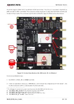
Page 11: ...USB Type C USB Type B U SIM1 Card Power Supply 5G M 2 Module DC DC Converter WLAN ETH Module U SIM2 Card CODEC SLIC Module J0803 J0501 J0502 B ANT4 ANT5 VCC GND Earphone Handset U0203 U0202 U0207 U0205 U0206 U0204 S0201 S0101 S0102 S0301 S1101 J0101 D0107 D0108 Figure 1 Top View and Component Placement of the EVB ...

Page 12: ... and Class C 1 8 V Support U SIM card insertion detection J0702 U SIM2 Interface Class B 3 0 V and Class C 1 8 V Support U SIM card insertion detection WLAN Ethernet Interfaces J0501 J0502 Support AF50T WLAN or RTL8111H RTL8125 Ethernet Audio Connector J0803 Support ALC5686 codec board or LE9643 SLIC board Earphone Interface J0801 3 5 mm earphone interface Used to test the analog audio function of...

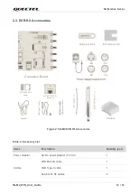
Page 13: ...H TE A Ethernet Headset USB Type C Cable USB Micro B Cable USB Flash Disk Soft Silicone Pad BS US BS CN Heatsink Figure 2 5G M2 EVB Kit Accessories Table 4 Accessory List Items Description Quantity pcs Power adapter AC DC power adapter 5 V 3 A 1 Cables USB Micro B cable 1 USB Type C cable 1 Sub 6 GHz RF cables 6 ...

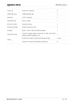
Page 14: ...A Codec module 1 RTL8111H TE A Ethernet module 1 Soft Silicone Pad Thermal conductive pad 1 Heatsink 60 mm 60 mm black anodized heatsink 1 Instruction sheet A sheet of paper giving instructions for EVB connection details of EVB accessories etc 1 Others Screws and copper cylinder for EVB assembling 4 pairs Screws for module and heatsink assembling 8 ...

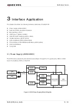
Page 15: ...2 J0803 PCIe interface to WLAN Ethernet Module J0501 J0502 Antenna interfaces Test points 3 1 Power Supply J0202 J0601 The EVB can be powered by an external power adapter through the 5 V power jack J0202 or USB Type C receptacle J0601 on the EVB S0201 Power Switch J0101 M 2 module 3 3 V U0207 DC DC U0206 DC DC U0204 DC DC J0501 J0502 WLAN ETH U0202 DC DC 3 8 V U0203 DC DC 1 95 V 0 95 V 1 35 V U020...

Page 16: ...ply Interfaces J0202 J0601 3 2 Switches Button and Status Indicators The EVB provides four switches S0101 S0201 S0301 S1101 one button S0102 and two indicators D0107 D0108 as shown in the following figure LOW level side HIGH level side LOW level side HIGH level side Figure 5 Switches Button and Status Indicators ...

Page 17: ...Pin 38 and 68 1 are connected to J0803 CODEC TE A S0301 2 LOW the module s Pin 20 22 24 and 28 are connected to J0501 and J0502 HIGH the module s Pin 20 22 24 and 28 are connected to J0803 S0301 3 Quectel internal use only S0301 4 LOW the module s PCIe is connected to J0401 USB Type B Connector HIGH the module s PCIe is connected to J0501 and J0502 S1101 S1101 1 Used to turn on off airplane mode L...

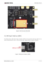
Page 18: ...the EVB 3 4 USB Type C Interface J0601 The EVB provides a USB 2 0 3 0 Type C interface J0601 for the connection with a host J0601 can be used for data transmission Also it can be used as power supply interface to power on the EVB J0601 USB Type C Interface Figure 7 USB Type C Interface J0601 ...

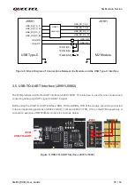
Page 19: ...ace 3 5 USB TO UART Interface J0901 J0902 The EVB provides a USB TO UART interface J0901 J0902 This interface is used for Linux console and converting debug log UART signal to USB 2 0 signal Before using the USB TO UART interface DBG_RXD and DBG_TXD of the module should be connected to the corresponding positions of J0902 2 RXD_1V8 and J0902 3 TXD_1V8 on the EVB respectively A connection example o...

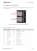
Page 20: ...C1 C2 C3 C4 C5 C6 C7 C8 C1 C2 C3 C4 C5 C6 C7 C8 CD CD Figure 10 Pin Assignments of U SIM Interfaces J0701 J0702 Table 6 Pin Definition of J0701 J0702 Pin No Pin Name I O Description C1 USIM_VDD PO U SIM card power supply C2 USIM_RST DO U SIM card reset C3 USIM_CLK DO U SIM card clock C4 RESERVED Not connected C5 GND Ground C6 VPP Not connected C7 USIM_DATA DIO U SIM card data C8 RESERVED Not conne...

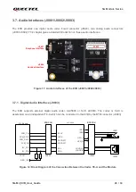
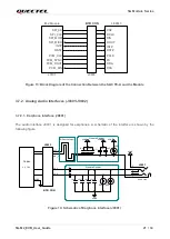
Page 21: ...rfaces of the EVB J0801 J0802 J0803 3 7 1 Digital Audio Interface J0803 The EVB supports external digital audio codec ALC5686 or SLIC LE9643 The codec or SLIC is assembled on an independent TE A which can be connected to the EVB by the BTB connector J0803 PCM_DIN PCM_DOUT PCM_SYNC PCM_CLK I2C_SCL I2C_SDA ALC5686 M 2 Module REG_1V8 2 2 K 2 2 K BCLK LRCK DACDAT1 ADCDAT1 SCL SDA IN2P IN2N LOUDL P LOU...

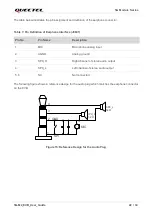
Page 22: ... 3 7 2 Analog Audio Interfaces J0801 J0802 3 7 2 1 Earphone Interface J0801 The audio interface J0801 is designed for earphones A schematic of the interface is shown by the following figure SPK_L MIC_N MIC_P 33 pF Close to Socket Differential layout 10 pF 10 pF 33 pF AGND Codec ALC5686 Close to Socket ESD ESD Audio Jack J0801 1 4 5 3 2 SPK_R 10 pF 33 pF 6 33 pF AGND 10 pF 4 7 μF BTB CON J0803 AGND...

Page 23: ...e following figure shows a reference design for the audio plug which matches the earphone connector on the EVB 2 1 MIC GND SW SPK_R SPK_L 3 4 32 Ω 32 Ω Figure 15 Reference Design for the Audio Plug Pin No Pin Name Description 1 MIC Microphone analog input 2 AGND Analog ground 3 SPK_R Right channel of stereo audio output 4 SPK_L Left channel of stereo audio output 5 6 NC Not connected ...

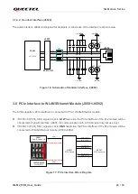
Page 24: ...02 The EVB supports a PCIe interface to connect with PC or WLAN Ethernet module If S0301 4 PCIE_SEL signal is set to LOW level side the PCIe interface of the M 2 module will be connected to Type B interface J0401 for communication with a PC Quectel internal use only If S0301 4 PCIE_SEL signal is set to HIGH level side the PCIe interface of the M 2 module will be connected to WLAN Ethernet module J...

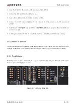
Page 25: ...8111H RTL8125 TE A RM500Q GL 5G M 2 Module Figure 18 Connections Between the EVB and a PC via Ethernet Functional verification steps 1 Set S0301 4 PCIE_SEL to HIGH level side 2 Insert an applicable module e g RM500Q GL which should be configured by AT Commands 2 into the M 2 connector J0101 and assemble the four antennas 2 The following AT commands are used to set the module into WLAN Ethernet fun...

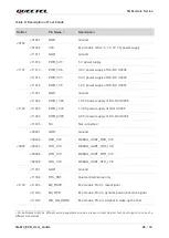
Page 26: ...the module 8 Until the green LED on RTL8111H TE A blinks it shows that the Ethernet PHY works normally 3 9 Antenna Interfaces The six antennas provided in the EVB kit are exactly the same They support 600 6000 MHz and can be randomly connected to the six antenna connectors ANT0 ANT5 on the EVB as shown in Figure 1 3 10 Test Points The EVB provides a series of test points helping to obtain the corr...

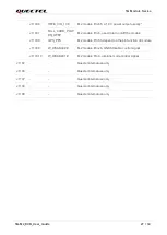
Page 27: ...f DC DC U0203 J1101 5 PWR_1V8 1 8 V power supply of DC DC U0207 J1104 J1104 1 GND Ground J1104 2 PWR_1V95 1 95 V power supply of DC DC U0206 J1104 3 PWR_1V35 1 35 V power supply of LDO U0205 J1104 4 PWR_0V95 0 95 V power supply of DC DC U0204 J1104 5 NC Not connected J0902 J0902 1 GND Ground J0902 2 RXD_1V8 DEBUG_UART_RXD_1V8 J0902 3 TXD_1V8 DEBUG_UART_TXD_1V8 J0902 4 DTR_1V8 DEBUG_UART_DTR_1V8 J0...

Page 28: ...off the module J1103 8 GPS_PPS M 2 module Pin 56 depend on the pin function of module J1103 9 W_DISABLE2 M 2 module Pin 26 GNSS disable control signal J1103 10 W_DISABLE1 M 2 module Pin 8 airplane mode control signal J1102 Quectel internal use only J1106 Quectel internal use only J1107 Quectel internal use only J1108 Quectel internal use only J1109 Quectel internal use only ...

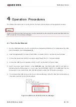
Page 29: ...e M 2 module to the EVB M 2 connector J0101 and then fix it with screws 3 Connect the power jack J0202 to a power supply through the 5 V 3 A power adapter 4 Connect the USB Type C receptacle J0601 to a PC via the USB 3 0 Type C cable 5 Switch the power switch S0201 to the PWR_ON side then PWR_LED D0107 will light on indicating that the EVB powers on In such case switch PWRKEY S0101 to the ON side ...

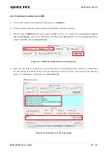
Page 30: ... COM24 as exemplified in Figure 20 and Baudrate such as 115200 bps and then click Open Port For more details about the usage of QCOM refer to document 2 Figure 21 COM Port and Baudrate Configurations 4 After the port opens successfully you can start the communication with the module via USB Send AT commands by QCOM and you will get responses from the module as shown by the following figure For det...

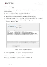
Page 31: ...ool QFlash provided by Quectel on the PC 3 Click the COM Port dropdown list and select the port number corresponding to Quectel USB DM port in the Device Manager e g COM20 as exemplified in Figure 20 and select Baudrate as illustrated by the following figure Figure 23 Firmware Upgrade Configurations 4 Click the Load FW Files button to select and load the firmware package 5 Click the Start button t...

Page 32: ...rn off the module Hardware method switch S0201 to PWR_OFF side to turn off the module Software method send AT QPOWD command to turn off the module which is preferred and safer since the module will log off from the network and save data before shutdown Pressing the RESET button i e triggering the RESET signal will lead to loss of all data in the modem and removal of system drivers It will also dis...

Page 33: ...ent consumption of the module in sleep mode at USB 3 0 when S0201 is on the PWR_ON side and that in sleep mode at USB 2 0 when S0201 is on the PWR_OFF side 3 Insert an applicable module e g RM500Q GL into the M 2 connector J0101 4 Connect an external power supply to the oval vias marked by the reference designators VCC and GND on the edge of the board to power the module independently Then turn on...

Page 34: ...ide 2 Quectel_QCOM_User_Guide 3 Quectel_RG50xQ RM5xxQ_Series_AT_Commands_Manual 4 Quectel_QFlash_User_Guide Abbreviation Description BTB Board to Board DI Digital Input DO Digital Output EVB Evaluation Board GNSS Global Navigation Satellite System I O Input Output LED Light Emitting Diode WLAN Wireless Local Area Network ETH Ethernet SLIC Subscriber Line Interface Circuit NC Not Connected ...

Page 35: ...mputer PCB Printed Circuit Board PCIe Peripheral Component Interconnect Express PO Power Output RefDes Reference Designator RF Radio Frequency UART Universal Asynchronous Receiver Transmitter USB Universal Serial Bus U SIM Universal Subscriber Identity Module ...

Reviews: