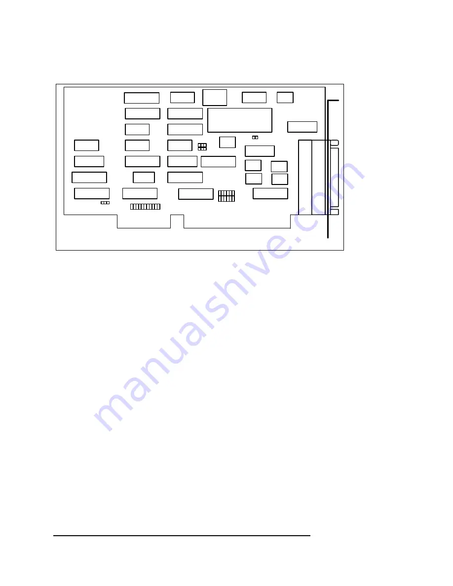
Figure 1 MPA-200 board drawing
Quatech, Inc.MPA-200
U1
U2
SW1
SW2
U3
U4
U5
U6
U7
U8
X1
U16
U9
U10
U11
U12
U13
U14
U15
U21
U17
J10J11
J5
J6
J4
CN2
CN1
U22
U23
U26
U18
U19
U20
U25
J8
J7
U29
U24
U28
3 Quatech Inc., MPA-200/300 Manual
Page 1: ...5 SYNCHRONOUS ADAPTER CARD for ISA compatible machines User s Manual QUATECH INC TEL 330 655 9000 5675 Hudson Industrial Parkway FAX 330 655 9010 Hudson Ohio 44236 http www quatech com INTERFACE CARDS FOR IBM PC AT AND PS 2 ...
Page 2: ......
Page 3: ...l Quatech Inc be liable for damages of any kind incidental or consequential in regard to or arising out of the performance or form of the materials presented herein and in the program s accompanying this document No representation is made regarding the suitability of this product for any particular purpose Quatech Inc reserves the right to edit or append to this document or the product s to which ...
Page 4: ...this document and every attempt has been made to ensure its accuracy and completeness In no event will Quatech Inc be liable for damages of any kind incidental or consequential in regard to or arising out of the performance or form of the materials presented in this document or any software programs that might accompany this document Quatech Inc encourages feedback about this document Please send ...
Page 5: ...n a particular installation If this equipment does cause harmful interference to radio or television reception which can be determined by turning the equipment off and on the user is encouraged to try to correct the interference by one or more of the following measures Reorient or relocate the receiving antenna Increase the separation between the equipment and receiver Connect the equipment into a...
Page 6: ...enerate an Interrupt 18 7 DIRECT MEMORY ACCESS 17 6 INTERRUPTS 15 5 ADDRESSING 14 4 6 J8 SYNCA to RLEN control 13 4 5 J7 Line Driver Control Selection 13 4 4 J11 Receive DMA Channel Selection 12 4 3 J10 Transmit DMA Channel Selection 11 4 2 J5 J6 Interrupt Level Selection 11 4 1 J4 Interrupt Configuration 11 4 JUMPER BLOCK CONFIGURATIONS 10 3 3 SCC Data Encoding Methods 9 3 2 Baud Rate Generator P...
Page 7: ...3 Quatech Inc MPA 200 300 Manual ...
Page 8: ...rts Direct Memory Access DMA and interrupts DMA channels 1 3 can be used for high data transfer rates while interrupt levels 2 7 10 12 and 14 15 are available for several interrupt sources On the MPA 200 communications is controlled by the SCC labeled U17 There are seven jumper blocks on the MPA 200 that allow the user to select such options as DMA channels interrupt levels and driver control If t...
Page 9: ...200 board drawing Quatech Inc MPA 200 U1 U2 SW1 SW2 U3 U4 U5 U6 U7 U8 X1 U16 U9 U10 U11 U12 U13 U14 U15 U21 U17 J10 J11 J5 J6 J4 CN2 CN1 U22 U23 U26 U18 U19 U20 U25 J8 J7 U29 U24 U28 3 Quatech Inc MPA 200 300 Manual ...
Page 10: ...page 17 and DIRECT MEMORY ACCESS on page 18 for detailed information on how to set the address IRQ and DMA levels 2 Turn off the power of the computer system in which the MPA 200 is to be installed 3 Remove the system cover according to the instructions provided by the computer manufacturer 4 Install the MPA 200 in any vacant expansion slot The board should be secured by installing the Option Reta...
Page 11: ... bits Odd even or no parity Times 1 16 32 or 64 clock modes Break generation and detection Parity overrun and framing error detection 2 Byte oriented Synchronous Communications Internal external character synchronization 1 or 2 sync characters in separate registers Automatic Cyclic Redundancy Check CRC generation detection 3 SDLC HDLC Bit Synchronous Communications Abort sequence generation and ch...
Page 12: ...ule is when accessing the transmit and receive data buffers These registers can be accessed with the two step process described or with a single read or write to the data port The following examples illustrate how to access the internal registers of the SCC Also Table 2 SCC read register description describes the read registers and Table 3 SCC write register descrip tion describes the write regist...
Page 13: ... without interrupts by reading the status of RR0 and then reading or writing data to the SCC buffers via CPU port accesses Interrupts on the SCC can be sourced from the receiver the transmitter or External Status conditions At the event of an interrupt Status can be determined then data can be written to or read from the SCC via CPU port accesses For block transfer mode DMA transfers accomplish da...
Page 14: ...l WR11 Miscellaneous transmitter receiver control bits NRZI NRZ FM coding CRC reset WR10 Master interrupt control and reset WR9 Transmit buffer WR8 HDLC enhancement register WR7 Sync character 2nd byte or SDLC Flag WR7 Sync character 1st byte or SDLC address field WR6 Transmitter initialization and control WR5 Transmit Receive miscellaneous parameters and codes clock rate stop bits parity WR4 Rece...
Page 15: ...he time constant is given below while Table 4 shows the time constants associated with a number of popular baud rates when using the standard MPA 200 9 8304 MHz clock Time_Const Clock_Frequency 2 Baud_Rate Clock_Mode 2 Where Clock_Frequency crystal frequency of 9 8304 MHz Clock_Mode value programmed in WR4 Baud_Rate desired baud rate Table 4 Time constants for common baud rates for 9 8304 Mhz Cloc...
Page 16: ...al phase locked loop DPLL that can be programmed to operate in NRZI or FM mode Also the SCC contains two features for diagnostic purposes controlled by bits in WR14 They are local loopback and auto echo For further information on these subjects or any others involving the SCC contact the manufacturer of the SCC being used for a complete technical manual Quatech Inc MPA 200 300 Manual 10 ...
Page 17: ...ification and cannot be shared Table 5 summarizes the jumper block selections for J4 To maintain 100 ISA bus compatibility J7 should be set in No Interrupt Sharing mode Table 5 Jumper Block J4 Selections 2 3 No Interrupt Sharing 1 2 Interrupt Sharing Pins Interrupt Function 4 2 J5 J6 Interrupt Level Selection Jumper blocks J5 and J6 select the interrupt level that the MPA 200 utilizes Inter rupt l...
Page 18: ...are available on the MPA 200 for DMA When selecting a DMA channel both the DMA acknowledge DACK and the DMA request DRQ for the appropriate channel need to be selected Table 8 summarizes the jumper block selections for J10 Table 8 Jumper block J10 selections 6 12 5 11 Channel 3 4 10 3 9 Channel 2 2 8 1 7 Channel 1 Pins DMA Channel Quatech Inc MPA 200 300 Manual 12 ...
Page 19: ...and J11 should never have the same pins connected This condition could result in damage to the system 4 5 J7 Line Driver Control Selection J7 controls the source for enabling and disabling the driver circuitry on the MPA 200 By selecting pins 1 2 the transmitters on the MPA 200 will always be enabled If the user wants the ability to enable and disable the transmitters pins 2 3 should be selected B...
Page 20: ... J8 SYNCA to RLEN control J8 controls the signal path from the RLEN bit in the Communications register to the SYNCA input to the SCC If J8 is installed the RLEN bit may be used to control the SYNCA pin when the SCC is in external SYNC mode Note the RLEN output is still effected when used to control the SYNCA pin Table 11 Jumper J8 Selections OUT RLEN IN SYNCA Jumper J8 Function Quatech Inc MPA 200...
Page 21: ...W1 allows the user to select the higher address signals A15 A8 SW2 allows the user to select the lower address signals A7 A3 The sixth position of SW2 is not used and can be ignored Figure 2 shows some examples of different base addresses Figure 1 Address switch selection examples ON ON ON O N 1 1 2 2 3 3 4 4 5 5 6 6 7 7 8 8 1 1 2 2 3 3 4 4 5 5 6 6 Base Address 300H Base Address 3F8H SW1 SW2 SW1 S...
Page 22: ...Register Base 5 Communications Register Base 4 SCC Control Port Channel B Base 3 SCC Data Port Channel B Base 2 SCC Control Port Channel A Base 1 SCC Data Port Channel A Base 0 Register Description Address Information on the internal registers of the SCC can be found in the chapter titled SCC GENERAL INFORMATION starting on page 4 The two onboard registers give the user additional options pertaini...
Page 23: ...SR must do to allow proper system operation 1 Do a software interrupt acknowledge to the SCC This is accom plished by reading the interrupt vector register status register 2 in channel B of the SCC The value supplied by this read can also be used to vector to the appropriate part of the ISR 2 Service the interrupt by reading the receiver buffer writing to the transmit buffer etc 3 Write a Reset Hi...
Page 24: ...hould only be used for DMA transfers if the user does not require a valid DTR signal at the connector This is due to the fact that when DTR REQA is used for DMA transfer it is not a valid handshake signal After programming the SCC for DMA one should enable the DMA on the MPA 200 by setting bit D2 of the configuration register Next the DMA on the SCC should be enabled and finally the DMA channel sh...
Page 25: ...of performing DMA requests on both transmit and receive Otherwise the third configuration should be used This configuration uses the W REQA pin of channel A for DMA request on trans mit and the W REQB pin of channel B for DMA request on receive This is done by clearing bit D0 and setting bit D1 of the configuration register Figure 3 shows a block diagram of the DMA circuitry on the MPA 200 When us...
Page 26: ...generating an interrupt whenever the Terminal Count TC signal is asserted Terminal Count is an indicator generated by the system s DMA controller which signals that the number of transfers programed into the DMA controller s transfer register have occurred This board feature only works when theinterrupt sharing feature is selected on jumper J4 Quatech Inc MPA 200 300 Manual 20 ...
Page 27: ...errupt The three sources are interrupt on terminal count INTTC interrupt from the SCC INTSCC and interrupt on Test Mode INTTM When the source is set that interrupt becomes enabled Below is the mapping for these bits INTTM 1 1 INTSCC 0 1 INTTC 1 0 Interrupts Disabled 0 0 Interrupt INTS0 INTS1 D3 DMREN DMA ON RECEIVE ENABLE When set logic 1 the signal from the SCC s receive DMA source is passed on t...
Page 28: ...MA SOURCE When set logic 1 this bit allows the source for transmit DMA to come from the DTR REQA pin of channel A on the SCC When cleared logic 0 the source for transmit DMA comes from the W REQA pin of channel A on the SCC NOTE If both D0 and D1 are cleared logic 0 then the transmit and receive DMA requests both come from the W REQA pin of channel A on the SCC Proper board function is not guarant...
Page 29: ... TM ST D0 D1 D2 D3 D4 D5 D6 D7 D7 TEST MODE STATUS DTE only read only This bit can read the status of the Test Mode signal on a DTE allowing the user to monitor this signal without generating any interrupts D6 Reserved always 0 D5 LOCAL LOOPBACK ENABLE DTE only When set logic 1 this bit allows the DTE to test the functioning of the DTE DCE interface and the transmit and receive sections of the loc...
Page 30: ... can only transmit its TCLK writing to this bit has no effect on a DCE D1 RECEIVER ENABLE If J7 is configured to allow the Communications Register to control the MPA 200 s receivers see Table 10 on page 14 then when D1 is set logic 1 the receivers are enabled and when D1 is cleared logic 0 the receivers are disabled D0 TRANSMITTER ENABLE If J7 is configured to allow the Communications Register to ...
Page 31: ...ttings of jumper block J7 See the chapter JUMPER BLOCK CONFIGURATIONS on page 11 for further informa tion on the configuration of this jumper block They both also have the ability to receive data and receive clock RCLK on channel B of the SCC This allows the user to transmit and receive on two different channels The differences between the MPA 200 s DTE configuration and its DCE configu ration inc...
Page 32: ...e clock RCLK from the SCC RTxC pins can be received on RRCLK or can be generated on the TRxCB pin of the SCC depend ing on RCKEN D3 of the communications register The DTE can not transmit its RCLK Figure 4 illustrates the clock circuitry of the MPA 200 for it s DTE configuration Figure 2 DTE Clock Configuration TRXCA RTXCA RTXCB RRCLK RTCLK TRXCB RCKEN TTCLK TCKEN RCLK TCLK The testing signals tha...
Page 33: ... DSR It can receive the signals Data Terminal Ready DTR and Ready to Send RTS All of the control signals are controlled through channel A of the SCC with the exception of the CD signal which is generated on channel B Depending on the value of TCKEN D2 of the communications register the DCE s transmit clock TCLK from the SCC s TRXCA pin can either be trans mitted on TTCLK or not used at all because...
Page 34: ...TTCLK TCKEN RCLK TCLK The Test Mode TM signal is always in the OFF condition and cannot be changed by the user The Local Loopback LL and Remote Loopback RL test signals are not implemented on the DCE Table 16 summarizes the signals on the DCE Quatech Inc MPA 200 300 Manual 28 ...
Page 35: ...and Figure 7 illustrate the pin outs for each of the connectors Table 15 DTE Connector Pin Definitions COMM REG D7 TEST MODE 25 TRXCA TTCLK 24 DTR REQA DTR 23 DCDB DSR 22 COMM REG D4 RLBK 21 DTR REQA DTR 20 RTSA RTS 19 COMM REG D5 LLBK 18 TRXC RRCLK 17 RXDA RXD 16 TRXCB RTCLK 15 TXDA TXD 14 CTSA CTS 13 TRXCB RTCLK 12 TRXCA TTCLK 11 DCDA CD 10 RTXC RRCLK 9 DCDA CD 8 DGND 7 DCDB DSR 6 CTSA CTS 5 RTS...
Page 36: ...nect 21 DCDA DSR 20 CTSA CTS 19 No Connect 18 TRXCA TTCLK 17 TXDA TXD 16 TRXCB RTCLK 15 RXDA RXD 14 RTSA RTS 13 TRXCB RTCLK 12 RTXC RRCLK 11 DTR REQB CD 10 TRXCA TTCLK 9 DTR REQB CD 8 DGND 7 DTR REQA DTR 6 RTSA RTS 5 CTSA CTS 4 TXDA TXD 3 RXDA RXD 2 No Connect 1 Source Signal Pin Quatech Inc MPA 200 300 Manual 30 ...
Page 37: ... CGND 1 TXD 2 RXD 3 RTS 4 CTS 5 DSR 6 DGND 7 CD 8 RRCLK 9 CD 10 TTCLK 11 RTCLK 12 CTS 13 Figure 5 MPA 200 DCE Output Connector 25 TEST MODE 24 RRCLK 23 DSR 22 DTR 21 N C 20 DSR 19 CTS 18 N C 17 TTCLK 16 TXD 15 RTCLK 14 RXD RXD 2 TXD 3 CTS 4 RTS 5 DTR 6 DGND 7 CD 8 TTCLK 9 CD 10 RRCLK 11 RTCLK 12 RTS 13 31 Quatech Inc MPA 200 300 Manual ...
Page 38: ...30 device it may be necessary to swap the conductors on the TXD and RXD signals 11 2 Null Modem Cables The MPA 200 does not use a standard asynchronous PC serial port connector pin out Typical off the shelf null modem cables cannot be used with this card Quatech Inc MPA 200 300 Manual 32 ...
Page 39: ...IRECTION To DCE This signal transfers the data generated by the DTE through the communication channel to one or more remote DCE data stations CIRCUIT BB RECEIVED DATA RxD CONNECTOR NOTATION RXD RXD DIRECTION From DCE This signal transfers the data generated by the DCE through the communications channel to one or more remote DTE data stations CIRCUIT DA TRANSMIT ELEMENT TIMING TxcLK DTE Source CONN...
Page 40: ... RTS CONNECTOR NOTATION RTS RTS DIRECTION To DCE This signal controls the data channel transmit function of the local DCE and on a half duplex channel the direction of the data transmission of the local DCE CIRCUIT CB CLEAR TO SEND CTS CONNECTOR NOTATION CTS CTS DIRECTION From DCE This signal indicates to the DTE whether the DCE is conditioned to transmit data on the communication channel CIRCUIT ...
Page 41: ...local DCE Note The local loopback and remote loopback signals are optional and are omitted from the DCE configuration of the MPA 200 Since testing will never occur for this configuration the test mode signal will always be in the OFF condition for the DCE These three test signals follow the EIA 423 A standard while the remaining signals follow the EIA 422 A standard CIRCUIT RL REMOTE LOOPBACK RL C...
Page 42: ...ON TEST MODE DIRECTION From DCE This signal indicates to the DTE that the DCE is in a test condition The DCE generates this signal when it has received a local loopback or remote loopback signal from the DTE Quatech Inc MPA 200 300 Manual 36 ...
Page 43: ...ivers EIA 422 MC3487 or compatible EIA 423 MC3488 or compatible EIA 485 75174 or compatible Receive buffers EIA 422 MC3486 or compatible EIA 423 75176 or compatible EIA485 75175 or compatible Transceivers EIA 422 75176 or compatible EIA 485 75176 or compatible I O Address range 0000H FFFFH Interrupt levels IRQ 2 7 10 12 14 15 Power requirements 12 36 25 12 36 25 5 1402 1248 Supply Voltage Volts IM...
Page 44: ...MPA 200 300 User s Manual Version 5 31 March 2004 Part No 940 0038 531 ...