QP-650 Plus Circuit Description
- 16 -
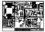
Fig. 5 AF and Signaling Circuit
CTC/CDC
Transmit:
CTC/CDC signaling produced by CTC_PLL pass a low pass filter and then enters
VCXO. CTC/CDC signaling produced by CTC_OUT pass a low pass filter and then mixed with AF
before enters VCO.
Receive:
Demodulated signal enters MCU after pass U200. MCU then judges whether CTC/CDC
matches the preset values or not. According the result, the out tone will be controlled by AFMUTE.
DTMF
Transmit:
The signal produced by MCU provides a TX and SP out tone, and is then applied to the
base band processing IC. The signal in mixed with the audio signal and goes to the VCO
。
AF
Transmit:
AF signal from MIC enters base band processed IC for amplification, pre-emphasis etc.
after being amplified. And then it enters VCO for modulation.
Receive:
Demodulated AF signal enters the base band processing IC for amplification,
de-emphasis etc. after being amplified. And then it enters AF power amplifier drived speaker.
Base band processed chip provides functions for processing signal as amplifying, filtering,
amplitude limiting.
6. Control system
The U611 CPU operates at 19.6608 MHz.
The block diagram of MCU control system is shown as following
:
Summary of Contents for QP-650 Plus
Page 1: ... 1 QP 650 Plus Service Manual Quantun Electronics LLC ...
Page 2: ... 2 Revised History No Date Decription Version Note 1 2010 3 9 Issue V0 1A ...
Page 60: ...QP 650 Plus PC Board View 60 PC Board View QP 650U Plus PCB Top Layer View 1 ...
Page 61: ...QP 650 Plus PC Board View 61 QP 650 Plus PCB Top Layer View 2 ...
Page 62: ...QP 650 Plus PC Board View 62 QP 650 Plus PCB Bottom Layer View 1 ...
Page 63: ...QP 650 Plus PC Board View 63 QP 650 Plus PCB Bottom Layer View 2 ...
Page 64: ...QP 650 Plus Block Diagram 64 Block Diagram ...
Page 65: ...QP 650 Plus Schematic Diagram 65 Schematic Diagram RF Section ...
Page 66: ...QP 650 Plus Schematic Diagram 66 AF Section ...
Page 67: ...QP 650 Plus Schematic Diagram 67 MCU Section ...


