background image

7


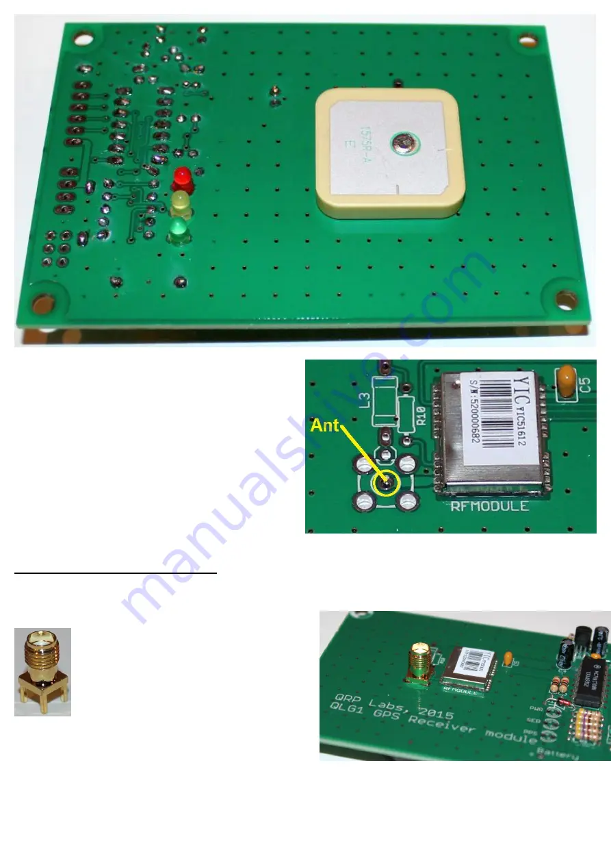
The patch antenna connection pin is not in the 
exact centre of the square patch. Please refer to 
the photograph (above). The connection pin should 
be furthest away from the through-hole 
components section of the PCB, as shown. The 
patch should be positioned on the solder side of the 
PCB.  

Insert the connection pin of the patch antenna into 
the centre-hole of the SMA socket. The photograph 
(right) illustrates the connection pin location. Solder 
the connection on the component side of the PCB. 

Remote active antenna installation 

If you decide to use an external active antenna, then do not install the supplied patch antenna. Instead, 
you can fit a SMA socket such as the one pictured 

here (left). 

Install the SMA socket on the PCB as 
shown in the photograph (right).  

In this case you may also need to supply 
power to the external active antenna. 

Then you should fit R10 and L3 (not supplied). 
Typically R10 should be 10 ohms, and L3 27nH (or a 
ferrite bead). You will need to solder a wire from the 
lower end of L3, to the SMA centre connector. This arrangement supplies power to the external antenna, 
from the RF Vcc supply output of the RF module. Note that it does not have short-circuit protection! 

Summary of Contents for QLG1

Page 1: ...ll ups or capacitors 2 Antenna The QLG1 GPS receiver kit can be built with two antenna options either an on board patch antenna or an externally mounted active antenna with SMA connector The module ca...

Page 2: ...ternal voltage regulation within the module The 74ACT logic family are perfect for the purposes of level conversion because the high voltage threshold specification for this family is below the 2 8V h...

Page 3: ...ors C1 0 1uF ceramic marking 104 C2 0 1uF ceramic marking 104 C3 22uF electrolytic C4 22uF electrolytic C5 0 1uF ceramic marking 104 4 3 Semiconductors IC1 74ACT08 14 pin DIP chip IC2 LM317LZ voltage...

Page 4: ...t could cause short circuits solder bridges to adjacent tracks Also look for joints where the solder has not correctly flowed into the joint i e adhered to the component lead and the PCB The QLG1 PCB...

Page 5: ...be too small to read so please refer to the parts placement diagram Battery Correct orientation of the battery is particularly critical Since the battery will already hold some charge when it arrives...

Page 6: ...component side of the board Additionally 2 x 3 header connection pads are provided in case you want to wire the LEDs to be mounted off board for example to fit into an enclosure or front panel header...

Page 7: ...emote active antenna installation If you decide to use an external active antenna then do not install the supplied patch antenna Instead you can fit a SMA socket such as the one pictured here left Ins...

Page 8: ...rge and easy to solder to The 6 way set of connections provides access to the full set of signals for general purpose use of this GPS receiver module Note that TXD is the serial data output of the mod...

Page 9: ...in the constellation can take around 1 hour So it is quite normal for performance of a GPS module to improve during the first hour after power up in terms of number of tracked satellites etc Until al...

Page 10: ...the QRP Labs YahooGroups forum if you have not already The forum members can provide support for any questions regarding issues and share your success stories too 9 Version History 0 10 Jun 2015 Firs...

Reviews: