Connection with the target circuit
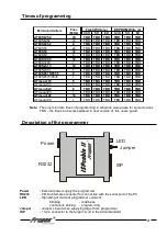
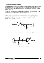
The connection to the target circuit should be realized through the attached 10-lead ribbon cable,
terminated with standard IDC plugs with 2.54 mm raster. In case of using another cable it should be
kept in mind that it should not be longer than 30 cm (~12 inches). The target device should be
equipped with a ISP connector with lead-out identical to that of the programmer ISP connector. We
connect the ISP bus lines with their corresponding ISP bus lines of the microcontroller as shown
in the figure below.
Connection with the
AT90S8515
microcontroller
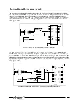
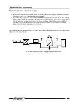
The LED signal can also serve to switching multiplexer the separating the signals MOSI, MISO,
SCK from the rest of system on time the programming. Solution such should be use in systems in
which to SPI BUS be connected different arrangements like Flash memory or RTC. It eliminates the
possibility of accidental record to these arrangements in time the programming the
microcontroller
.
Signal LED in programming moment switch to low level. The connection using multiplexer is shown
in the figure below.
Connection with the
AT90S8515
microcontroller with multiplexer
6
1
2
3
4
5
6
A
B
C
D
6
5
4
3
2
1
D
C
B
A
Title
Number
R ev isio n
Size
B
Date:
4-Ju l-20 0 2
Sheet o f
File:
C:\Mo je d ok u men ty \us er\Evb _at90.d d b
Drawn By:
R ESET
9
XTAL2
18
XTAL1
19
GND
20
OC 1B
2 9
ALE
3 0
ICP
3 1
VC C
4 0
PC0 /A8
2 1
PC1 /A9
2 2
PC2 /A1 0
2 3
PC3 /A1 1
2 4
PC4 /A1 2
2 5
PC5 /A1 3
2 6
PC6 /A1 4
2 7
PC7 /A1 5
2 8
PD0/RXD
10
PD1/TXD
11
PD2/INT0
12
PD3/INT1
13
PD4
14
PD5/OC 1 A
15
PD6/W R
16
PD7/R D
17
PB0/T0
1
PB1/T1
2
PB 2/AIN0
3
PB 3/AIN1
4
PB4/SS
5
PB5/MOSI
6
PB6/MISO
7
PB 7/SC K
8
PA0 /AD0
3 9
PA1 /AD1
3 8
PA2 /AD2
3 7
PA3 /AD3
3 6
PA4 /AD4
3 5
PA5 /AD5
3 4
PA6 /AD6
3 3
PA7 /AD7
3 2
AT9 0S851 5
X0
1 2
X1
1 3
Y0
2
Y1
1
Z0
5
Z1
3
INH
6
A
1 1
B
1 0
C
9
X
1 4
Y
1 5
Z
4
4 0 53 /7 4 HC 40 53
PB6
PB7
PB5
1
2
3
4
5
6
7
8
9
1 0
JP2
ISP Head er
RST
ISP ACTIVE
47 0R - 1 k
VTG
VTG
VTG
MOSI
LED
C LK
MISO
Reset circuit
ISP m ultiplexer
1
2
3
4
5
6
A
B
C
D
6
5
4
3
2
1
D
C
B
A
Title
Numb er
R ev isio n
Size
B
Date:
4 -Jul-20 0 2
Sh eet of
File:
C:\Moje dok umen ty \us er\Ev b_at9 0.dd b
Drawn By :
R ESET
9
XTAL2
1 8
XTAL1
1 9
GND
2 0
OC 1 B
29
ALE
30
ICP
31
VC C
40
PC0 /A8
21
PC1 /A9
22
PC2 /A1 0
23
PC3 /A1 1
24
PC4 /A1 2
25
PC5 /A1 3
26
PC6 /A1 4
27
PC7 /A1 5
28
PD0 /RXD
1 0
PD1 /TXD
1 1
PD2 /INT0
1 2
PD3 /INT1
1 3
PD4
1 4
PD5 /OC 1A
1 5
PD6/W R
1 6
PD7/R D
1 7
PB0 /T0
1
PB1 /T1
2
PB 2 /AIN0
3
PB 3 /AIN1
4
PB4 /SS
5
PB5 /MOSI
6
PB6 /MISO
7
PB 7 /SC K
8
PA0 /AD0
39
PA1 /AD1
38
PA2 /AD2
37
PA3 /AD3
36
PA4 /AD4
35
PA5 /AD5
34
PA6 /AD6
33
PA7 /AD7
32
AT9 0 S85 15
1
2
3
4
5
6
7
8
9
10
JP2
ISP Head er
RST
ISP ACTIVE
47 0 R - 1 k
VTG
VTG
VTG
MOSI
LED
C LK
MISO
Reset circuit


