EL320.256-FD7 Operations Manual (020-0353-00A)
6
Connectors
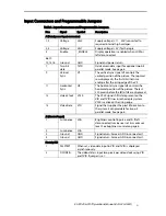
Table 2. Connectors.
J1
16-pin header
ODU 511.066.003.016 or eq.
Mating
ODU
517.065.003.016
or
eq.
J2
4-pin header
Hirose DF1–4P–2.5 DSA or eq.
Mating
Hirose DF1–4S–2.5 R 24 or eq.
Protector Hirose
DF1–4A
1.33
Control basics
The EL panel has 320 transparent column electrodes crossing 256 row
electrodes in an X-Y fashion. Light is emitted when an AC voltage is applied at
a row-column intersection. The display operation is based on the symmetric,
line at a time data addressing scheme which is synchronized by the external
VS, HS, and video clock input signals. The signal inputs are HCT compatible
with 100
Ω
series resistors.
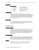
Power Input
The input voltages needed are the +5 V input (Vcc1) for the logic and the
+11…+30V input (Vcc2) for the DC/DC converter. All high voltages required
for display glass access are generated internally.
Display Features
Luminance Control
The luminance of the display can be adjusted from below 10% up to full
brightness by a 50 k
Ω
external logarithmic potentiometer between LCa and
LCb control inputs (J2/1 and /2). The control function is achieved by sinking a
small current from LCa to LCb (when open, the voltages are at 5V and 0V
respectively). If the two inputs are left disconnected, the brightness is at its
maximum level.
Two-Bits-Parallel
For reduction of data clock frequency, it is possible to input the data of two
pixels per pixel clock. This feature is selected with DCONFIG jumper (PS1/2). If
the jumper is set, data for even columns is input in VID and data for odd
columns is input in TVID. If jumper is open, data is input normally to VID only.
Self Test
When SELFEST jumper (PS1/1) is set, the video data at VID and TVID are
displayed asynchronously without the use of any timing signals.


