background image

23

5

6

7

8

F

E

D

C

B

A

5

6

7

8

GM-D505/XH/EW

R

609

RD1/4PU472J

R

610

RD1/4PU103J

R

611

RD1/4PU472J

R

612

RD1/4PU101J

R

613

RD1/4PU221J

R

614

RD1/4PU102J

R

615

RD1/4PU104J

R

616

RS1/16S101J

R

619

RS1/16S202J

R

620

RS1/16S103J

R

621

RS1/16S102J

R

622

RS1/16S153J

R

623

RS1/16S105J

R

625

RD1/4PU332J

R

626

RD1/4PU332J

R

627

RS1/16S472J

R

628

RS1/16S472J

R

629

RD1/4PU272J

R

630

RD1/4PU272J

R

631

RD1/4PU272J

R

632

RS1/16S472J

R

633

RS1/2PMF560J

R

634

RS1/2PMF560J

R

635

RS1/2PMF560J

R

636

RS1/2PMF560J

R

637

RS1/2PMF560J

R

638

RS1/2PMF560J

R

639

RS1/2PMF560J

R

640

RS1/2PMF560J

R

641

RD1/4PU472J

R

642

RD1/4PU472J

R

643

RS1/2PMF220J

R

645

RS1/2PMF100J

R

646

RS1/2PMF100J

R

647

RD1/4PU472J

R

648

RD1/4PU472J

R

649

RS1/2PMF220J

R

650

RS1/16S102J

R

654

RD1/4PU223J

R

655

RD1/4PU223J

R

656

RD1/4PU223J

R

657

RS1/16S124J

R

658

RS1/16S472J

R

659

RS1/16S472J

R

660

RS1/16S123J

R

661

RS1/16S182J

R

662

RS1/16S223J

R

663

RS1/16S182J

R

664

RS1/16S153J

R

665

RS1/2PMF100J

R

666

RS1/2PMF100J

R

667

RS1/16S272J

R

801

RS1/16S471J

R

802

RS1/16S471J

R

803

RS1/16S223J

R

804

RS1/16S223J

R

805

RN1/10SE1002D

R

806

RN1/10SE1002D

R

807

RN1/10SE1002D

R

808

RN1/10SE1002D

R

809

RN1/10SE1002D

R

810

RN1/10SE1002D

R

811

RN1/10SE1002D

R

812

RN1/10SE1002D

R

813

RS1/16S562J

R

814

RS1/16S562J

R

815

RS1/16S562J

R

816

RS1/16S562J

R

817

RS1/16S511J

R

818

RS1/16S511J

R

819

RS1/16S514J

R

820

RS1/16S514J

R

831

RS1/16S471J

R

832

RS1/16S471J

R

833

RS1/16S223J

R

834

RS1/16S223J

R

835

RN1/10SE1002D

R

836

RN1/10SE1002D

R

837

RN1/10SE1002D

R

838

RN1/10SE1002D

R

839

RN1/10SE1002D

R

840

RN1/10SE1002D

R

841

RN1/10SE1002D

R

842

RN1/10SE1002D

R

851

RS1/16S471J

R

852

RS1/16S471J

R

853

RS1/16S223J

R

854

RS1/16S223J

R

855

RN1/10SE1002D

R

856

RN1/10SE1002D

R

857

RN1/10SE1002D

R

858

RN1/10SE1002D

R

859

RN1/10SE1002D

R

860

RN1/10SE1002D

R

861

RN1/10SE1002D

R

862

RN1/10SE1002D

R

901

RD1/4PU473J

R

902

RD1/4PU473J

R

903

RD1/4PU473J

R

904

RD1/4PU473J

R

905

RD1/4PU473J

R

906

RD1/4PU473J

R

917

RD1/4PU104J

R

918

RD1/4PU472J

R

919

RD1/4PU103J

R

920

RD1/4PU222J

R

921

RD1/4PU472J

R

922

RD1/4PU221J

R

923

RD1/4PU222J

R

924

RD1/4PU563J

R

930

RD1/4PU331J

R

931

RD1/4PU331J

CAPACITORS

C

101

CFTNA104J50

C

102

CFTNA104J50

C

105

CFTNA474J50

C

106

CFTNA474J50

C

151

CFTNA184J50

C

152

CFTNA184J50

C

153

CFTNA224J50

C

154

CFTNA224J50

C

201

CEAT100M50

C

202

CEAT100M50

C

203

CEAT100M50

C

204

CEAT100M50

C

301

CCSRCH121J50

C

302

CCSRCH121J50

C

351

CCSRCH470J50

=====Circuit Symbol and No.===Part Name

Part No.

---

------

------------------------------------------

-------------------------

=====Circuit Symbol and No.===Part Name

Part No.

---

------

------------------------------------------

-------------------------

Summary of Contents for GM-D505

Page 1: ... NV Haven 1087 Keetberglaan 1 9120 Melsele Belgium PIONEER ELECTRONICS ASIACENTRE PTE LTD 253 Alexandra Road 04 01 Singapore 159936 C PIONEER CORPORATION 2003 K ZZB MAY 2003 Printed in Japan ORDER NO CRT3076 5 CHANNEL POWER AMPLIFIER GM D505XH EW XR EW Service Manual GM D505 XH EW GM D505XH ES XR ES For details refer to Important symbols for good services ...

Page 2: ... to proper portions by the appropriate amount For replacement parts or tools the prescribed ones should be used 4 Shipping mode and shipping screws To protect the product from damages or failures that may be caused during transit the shipping mode should be set or the shipping screws should be installed before shipping out in accordance with this manual if necessary 1 Product safety You should con...

Page 3: ...nel A B 100 W 4 4 Ω Channel SUB 300 W 1 4 Ω 600 W 1 2 Ω Continuous power output 65 W 4 4 Ω 225 W 1 4 Ω 56 W 4 4 Ω 350 W 1 2 Ω DIN45324 B 14 4 V Load impedance 4 Ω Channel A B 4 8 Ω allowable Channel SUB 2 8 Ω allowable Frequency response Channel A B 10 40 000 Hz 0 dB 1 dB Channel SUB 5 240 Hz 0 5 dB 3 dB Signal to noise ratio 95 dB IEC A network Distortion Channel A B 0 01 10 W 1 kHz Channel SUB 0...

Page 4: ...4 1 2 3 4 1 2 3 4 F E D C B A GM D505 XH EW 2 EXPLODED VIEWS AND PARTS LIST 2 1 PACKING ...

Page 5: ...RD0233 8 3 Warranty Card HRY1157 Not used 9 Core HTX0003 HTX0003 10 Polyethylene Bag HEG0025 HEG0025 11 Lock Tie HNV0025 HNV0025 PACKING SECTION PARTS LIST NOTE Parts marked by are generally unavailable because they are not in our Master Spare Parts List Screws adjacent to mark on the product are used for disassembly For the applying amount of lubricants or glue follow the instructions in this man...

Page 6: ...6 1 2 3 4 1 2 3 4 F E D C B A GM D505 XH EW 2 2 EXTERIOR A B C ...

Page 7: ...r CN103 HKS0005 30 Clip HNC0054 31 Holder HNC0143 32 Holder HNC0144 33 Spacer HNM0006 34 Insulator HNM0125 35 Insulator HNM0126 36 Bar HNR0124 37 Heat Sink HNR0201 38 Heat Sink HNR0202 39 Heat Sink HNR0203 40 Screw PPZ30P120FZK 41 Screw VBZ30P110FZK 42 Network Unit HWG0030 43 Connector CN102 HKS0004 44 Clip HNC0054 45 Screw PBB30P140FMC 46 Screw PPZ30P120FZK 47 Light Pipe Unit HXA0383 48 IC IC501 ...

Page 8: ...rvice parts be sure to refer to EXPLODED VIEWS AND PARTS LIST or ELECTRICAL PARTS LIST A a A B B HPF SWITCH A HPF SWITCH BFC SWITCH 100K B 10K A 10K A 20K E B NETWORK PCB 1 2 B NETWORK PCB 2 2 A Freq A Freq A Gain A Gain B Freq B Freq B Freq B Freq B Gain B Gain Sub Freq Sub Freq Sub Gain Sub Gain 1 1 2 8 1 2 3 4 1 2 3 4 F E D C B A GM D505 XH EW ...

Page 9: ...dicates the importance of the safety factor of the part Therefore when replacing be sure to use parts of identical designation Symbol indicates a resistor No differentiation is made between chip resistors and discrete resistors NOTE Symbol indicates a capacitor No differentiation is made between chip capacitors and discrete capacitors NETWORK UNIT Consists of NETWORK PCB CONNECTOR PCB HEK0025 HEK0...

Page 10: ... F E D C B A GM D505 XH EW A a A b A a A a A b B 1 2 B HPF SWITCH A HPF SWITCH 10K B 10K B B NETWORK PCB 1 2 A Freq A Freq A Gain A Gain B Freq B Freq B Freq B Freq B Gain B Gain Sub Freq Sub Freq Sub Gain Sub Gain 20K E ...

Page 11: ...11 5 6 7 8 F E D C B A 5 6 7 8 GM D505 XH EW A a A b A a A a A b C B 3 4 5 6 BFC SWITCH 100K B B NETWORK PCB 2 2 Sub Freq Sub Gain 1 1 2 ...

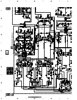
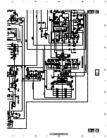
Page 12: ...12 1 2 3 4 1 2 3 4 F E D C B A GM D505 XH EW A a A b A b 1 2 A AMP UNIT 2 2 3 ...

Page 13: ...ts indicates the importance of the safety factor of the part Therefore when replacing be sure to use parts of identical designation Symbol indicates a resistor No differentiation is made between chip resistors and discrete resistors NOTE Symbol indicates a capacitor No differentiation is made between chip capacitors and discrete capacitors NETWORK UNIT Consists of NETWORK PCB CONNECTOR PCB HEK0025...

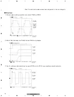
Page 14: ...m measured at TP638 and TP639 Waveforms Note The encircled numbers denote measuring pointes in the circuit diagram 2 BRem TP624 Stand by line TP253 Mute line TP254 timing diagram 3 Class D switching audio waveform at no signal TP413 and or TP414 same waveform on both test points ...

Page 15: ...15 5 6 7 8 F E D C B A 5 6 7 8 GM D505 XH EW ...

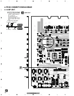
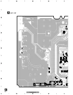
Page 16: ...parts mounted on this PCB include all necessary parts for several destination For further information for respective destinations be sure to check with the schematic dia gram 2 Viewpoint of PCB diagrams BFC B CN102 16 1 2 3 4 1 2 3 4 F E D C B A GM D505 XH EW 4 PCB CONNECTION DIAGRAM 4 1 AMP UNIT ...

Page 17: ...17 5 6 7 8 F E D C B A 5 6 7 8 GM D505 XH EW A SIDE A AR AR AL AL BR BR BL BL SR SL C CN702 C CN701 C CN703 ...

Page 18: ...18 1 2 3 4 1 2 3 4 F E D C B A GM D505 XH EW A A AMP UNIT AR AR AL AL BR BR BL BL SR TP638 TP639 TP624 ...

Page 19: ...19 5 6 7 8 F E D C B A 5 6 7 8 GM D505 XH EW A SIDE B SR SL TP414 TP413 TP253 TP254 ...

Page 20: ...20 1 2 3 4 1 2 3 4 F E D C B A GM D505 XH EW 4 2 NETWORK PCB B B NETWORK PCB B NETWORK PCB SIDE A SIDE B C CONNECTOR PCB C CONNECTOR PCB SIDE A SIDE B C A CN103 A A A 4 3 CONNECTOR PCB ...

Page 21: ...Q 909 Transistor KSA812 D 201 Diode 1SS133 D 202 Diode 1SS133 D 301 Diode HZS7L B2 D 302 Diode HZS7L B2 D 303 Diode HZS7L B2 D 304 Diode HZS7L B2 D 601 Diode RM4Z LFJ4 D 602 Diode HZS7L B2 D 603 Diode 1SS133 D 604 Diode RM4Z LFJ4 D 606 Diode 1SS133 D 607 Diode 1SS133 D 608 Diode 1SS133 D 609 Diode 1SS133 D 610 Diode FML22R D 611 Diode FML22S D 612 Diode HZS16L 1 D 613 Diode HZS16L 1 D 614 Diode ER...

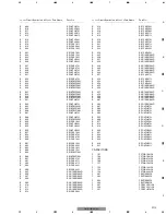
Page 22: ... RD1 4PU102J R 404 RD1 4PU102J R 405 RD1 4PU512J R 406 RD1 4PU512J R 407 RS1 16S474J R 408 RS1 16S474J R 409 RS1 16S472J R 410 RS1 16S472J R 411 RS1 16S101J R 412 RS1 16S101J R 413 RS1 16S153J R 414 RS1 16S153J R 415 RD1 4PU560J R 416 RD1 4PU560J R 417 RD1 4PU270J R 418 RD1 4PU270J R 419 RD1 4PU220J R 420 RD1 4PU220J R 421 RD1 4PU240J R 422 RD1 4PU240J R 423 RS1 16S474J R 424 RS1 16S474J R 425 RS1...

Page 23: ...E1002D R 809 RN1 10SE1002D R 810 RN1 10SE1002D R 811 RN1 10SE1002D R 812 RN1 10SE1002D R 813 RS1 16S562J R 814 RS1 16S562J R 815 RS1 16S562J R 816 RS1 16S562J R 817 RS1 16S511J R 818 RS1 16S511J R 819 RS1 16S514J R 820 RS1 16S514J R 831 RS1 16S471J R 832 RS1 16S471J R 833 RS1 16S223J R 834 RS1 16S223J R 835 RN1 10SE1002D R 836 RN1 10SE1002D R 837 RN1 10SE1002D R 838 RN1 10SE1002D R 839 RN1 10SE100...

Page 24: ...A105J50 C 508 CFTLA105J50 C 509 CFTLA105J50 C 510 CFTLA105J50 C 511 CKSRYB471K50 C 512 CKSRYB471K50 C 513 CKSRYB471K50 C 514 CKSRYB471K50 C 517 CFTNA333J50 C 518 CFTNA333J50 C 519 CQMA102J50 C 520 CQMA102J50 C 551 CEAT220M50 C 552 CEAT220M50 C 553 CEAT101M50 C 554 CEAT101M50 C 555 CEAT220M50 C 556 CEAT220M50 C 557 CFTLA105J50 C 558 CFTLA105J50 C 559 CFTLA105J50 C 560 CFTLA105J50 C 561 CKSRYB471K50...

Page 25: ...RYB472K50 C 856 CKSRYB472K50 C 857 CCSRCH470J50 C 858 CCSRCH470J50 C 859 CCSRCH470J50 C 860 CCSRCH470J50 C 901 220µF 10V HCH0012 NETWORK UNIT Consists of NETWORK PCB CONNECTOR PCB Unit Number HWG0030 Unit Name Network Unit MISCELLANEOUS IC 131 IC NJM2068MD IC 331 IC NJM2068MD S 131 Switch A HPF HSH0004 VR 131 Variable Resistor 20kΩ E A Freq CCS1266 VR 201 Variable Resistor 10kΩ A Sub Gain CCS1265 ...

Page 26: ...Y 1 Fig 1 Remove the five screws Removing the Case Fig 1 Case 2 Remove the four screws 1 3 1 1 1 1 Fig 2 1 Removing the Amp Unit Fig 2 Remove the five screws and then remove the Amp Unit 3 Remove the three screws 2 Remove the three Fuses and then remove the Case 2 2 2 2 3 3 Fuse Amp Unit 1 1 1 1 1 ...

Page 27: ...27 5 6 7 8 F E D C B A 5 6 7 8 GM D505 XH EW 7 1 2 CONNECTOR FUNCTION DESCRIPTION ...

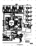
Page 28: ...5 Vs VRefl 24 SNL1 23 SNL2 22 GNLS 21 GNL 52 2 5V 51 NC 50 INR 49 INR 48 NC 47 NC 46 INL 45 INL 44 NC 43 NC 42 Vs Low 41 NC 40 5V DIG 39 NC 38 NTC 37 THWext 36 THWint 35 NC 34 O0 15 33 I OFCLK SGND 53 2 5V 54 MUTE 55 STBY 56 Feed R in 57 Vs3 58 Vs4 59 Vs VRefr 60 SNR1 61 SNR2 62 GNRS 63 GNR 64 TDA7570 TDA7294V MUTE STBY THERMAL SHUTDOWN S C PROTECTION 2 3 4 10 9 1 8 15 6 14 13 7 1 3 4 7 9 11 13 15...

Page 29: ...signal The Vd signal has a fundamental frequency equal to that of the modulation frequency Fm the frequency of the modu lation signal Vm but will also contain the input signal and a band of frequency components around the modulation frequency The original signal Fvin is selected with a low pass filter cutting the high frequencies around the modulation frequen cy Fm Fvin original signal Fc cut off ...

Page 30: ...eo with max output of 4 V or more adjust level to match the car stereo output level When you want to boost bass turn the bass level control clockwise Power Indicator The power indicator lights when the power is switched on BFC Beat Frequency Control Switch If you hear a beat while listening to an MW LW broadcast with your car stereo change the BFC switch using a small standard tip screwdriver HPF ...

Reviews: