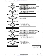
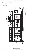
DVR-640H-S
111
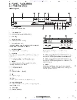
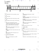
5
7
8
5
6
7
8
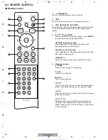
C
D
F
A
B
E
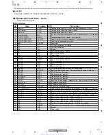
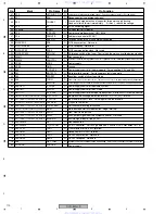
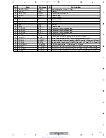
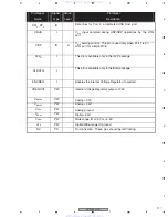
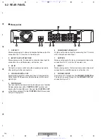
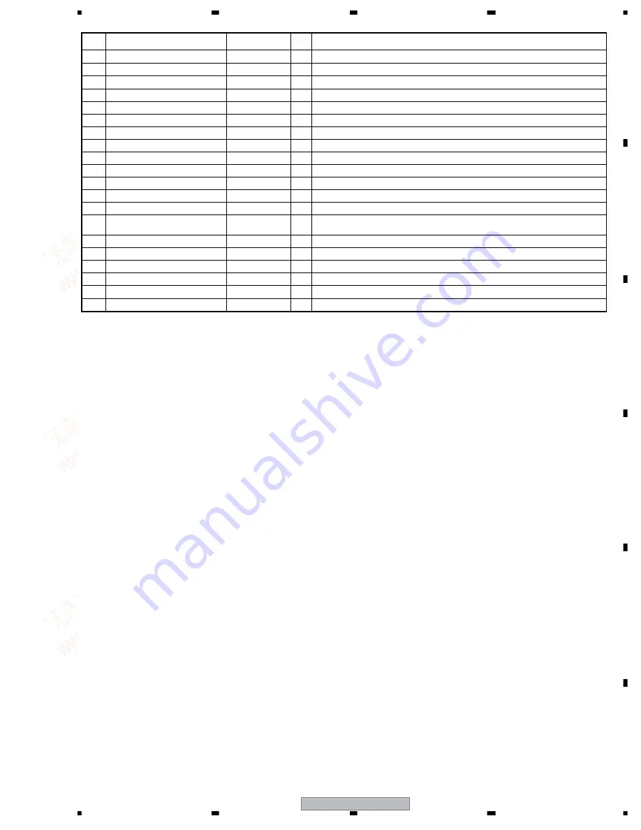
No.
Mark
Pin Name
I/O
Pin Function
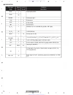
81
PB6/CVD/CSYNC
CVBSIN
I
Input video for data slicer 1.0Vpp
82
VSSVCO
GND
−
Ground
83
PB4/FILTSLC
FILTSLC
I
External filter for slicer PLL
84
VDDVCO
VDDVCO
−
Power supply
85
PB2
NC
O
Non connection
86
PB1
NC
O
Non connection
87
PB0/DS1FLD
NC
O
Non connection
88
VSS3
GND
−
Ground
89
VDD3
VDD3
−
Power supply
90
PC7/DBGP2
DBGP2
O/D Control port for on-chip debugger
91
PC6/DBGP1
DBGP1
O/D Control port for on-chip debugger
92
PC5/DBGP0
DBGP0
O/D Control port for on-chip debugger
93
PC4/AN11
C/N
AI C/N detection of BS-IF
94
PC3/AN10
BS15IN
I
Antenna power supply detection of the BS-OUT terminal
There is power supply with L. There is no power supply with H
95
PC2/AN9
BS15SRT
I
Antenna power supply short-circuit detection of the BS-IN terminal L: Short-circuit, H: Normal
96
PC1/AN8
BS15ON
O
Antenna power supply control to the BS-IN terminal L: Power OFF, H: Power ON
97
PC0/OCSYNC
P_SAVEBS
O
BS RF through control L: Not through, H: Through
98
PA0/SO7
SD_TTOM
O
System controller communication data line From tuner controller to system controller
99
PA1/SI7/SB7
SD_MTOT
I
System controller communication data line From system controller to tuner controller
100 PA2/SCK7
SCK_MTOT
I
System controller communication clock From system controller to tuner controller
www. xiaoyu163. com
QQ 376315150
9
9
2
8
9
4
2
9
8
TEL 13942296513
9
9
2
8
9
4
2
9
8
0
5
1
5
1
3
6
7
3
Q
Q
TEL 13942296513 QQ 376315150 892498299
TEL 13942296513 QQ 376315150 892498299


