1. CIRCUIT DESCRIPTIONS
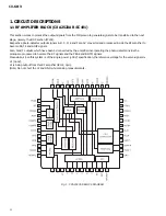
1.1 RF AMPLIFIER BLOCK (CXA2523AR : IC101)
This section works to process the output signals from the MD pickup to generate signals to be transferred to the next
stage, namely, the DSP section (IC201).
Respective photo-detector output signals A, B, C, D, E and F are I-V converted and processed inside the RF amplifier to
become FE, TE and ADIP signals.
Also, I and J outputs which have been I-V converted by the amplifier incorporating the photo-detector inside the
pickup are processed to become the RF signals and the PEAK and BOTM signals.
Meanwhile, since this system is of the single power (+3.3V) specification, the reference voltage for the servo-signals is
Vc (1.65V).
Vc is being output from this RF amplifier (IC101, 3pin).
(Note) Do not short the Vc and GND while making measurements.
2
CX-683
Fig. 1 : CXA2523AR BLOCK DIAGRAM


