-
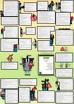
LCD module troubleshooting
1
No images
Normal signal is obtained at
each terminal of CN001?
Circuit current flows normally?
Go to Item
2
No power.
Check the CN001 , inputconnecting
flexible cables and its periphery.
Video signal is obtained at R654(75 ohms)?
5V is obtained at Pin-43 of Q201(IR3Y29BM)?
7.5V is obtained at Pin-23 of Q201(IR3Y29BM)?
POLC(Common reversing signal and square wave)
is obtained at Pin-32 of Q201(IR3Y29BM)?
POLS(Reflection reversing signal and square wave)
is obtained at Pin-33 of Q201(IR3Y29BM)?
18.5V is obtained at JP851 , -12V is obtained
at JP852 , 3.3V is obtained at JP853 ,
5.3V is obtained at JP809 and
7.5V is obtained at JP808?
Sync signal is obtained at Pin-36 of Q201(IR3Y29BM)?
Check Pin-13 , 14 of Q003
(Gate array) and its periphery.
Check Pin-3 of Q201 ,
C204 and its periphery.
Yes
Yes
Yes
Yes
Yes
Yes
Yes
Yes
No
No
No
No
No
No
No
No
Go to Item
2
No power.
Go to Item
2
No power.
Check CN001 , inputconnecting
flexible cables and its periphery.
Go to Item
3
Out of Sync.
Video signal is obtained at
Pin-3 of Q201(IR3Y29BM)?
49
AVX-7300
6. ADJUSTMENT
There is no information to be shown in this chapter.
7. GENERAL INFORMATION
7.1 DIAGNOSIS
7.1.1 TROUBLESHOOTING
Summary of Contents for AVX-7300/ES
Page 4: ...4 AVX 7300 2 2 EXTERIOR 1 3 A E ...
Page 6: ...6 AVX 7300 G 2 3 EXTERIOR 2 3 C F ...
Page 8: ...8 AVX 7300 B 2 4 EXTERIOR 3 3 D ...
Page 19: ...19 AVX 7300 ...
Page 21: ...21 AVX 7300 5 6 7 8 A B C D 5 6 7 8 C RELAY UNIT A CN101 C ...
Page 25: ...25 AVX 7300 ...
Page 26: ...26 AVX 7300 A 1 2 3 4 B C D 1 2 3 4 H C CN1101 3 8 VIDEO SCHEMATIC ...
Page 27: ...27 AVX 7300 5 6 7 8 A B C D 5 6 7 8 H H VIDEO SCHEMATIC ...
Page 29: ...29 AVX 7300 5 6 7 8 A B C D 5 6 7 8 SIDE A A E E CN1901 ...
Page 30: ...30 AVX 7300 A 1 2 3 4 B C D 1 2 3 4 A CONTROL PCB A AV BUS IP OUT IP IN OPT OUT SPEAKER ...
Page 31: ...31 AVX 7300 5 6 7 8 A B C D 5 6 7 8 SIDE B A IC Q FRONT RGB CORD ...
Page 33: ...33 AVX 7300 1 2 3 4 A B C D 1 2 3 4 IC Q C SIDE B RELAY UNIT C ...
Page 38: ...38 AVX 7300 A 1 2 3 4 B C D 1 2 3 4 4 7 VIDEO SCHEMATIC H VIDEO SCHEMATIC H C CN1101 ...


