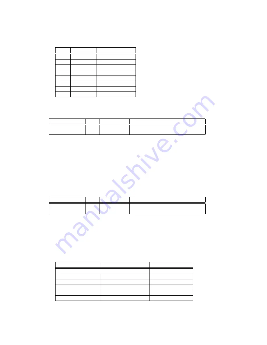
PiKRON ULAD 31 User Manual Download Page 5

Gain

Mode value

Input voltage range

1

×

0

±

10 V

2

×

1

±

5 V

4

×

2

±

2.5 V

8

×

3

±

1.25 V

16

×

4

±

625 mV

32

×

5

±

300 mV

64

×

6

±

150 mV

128

×

7

±

75 mV

3.1.6

ADC Input Terminals Selection

Name

R/W

Type

Function

CHA_INMUX

R/W

u2
<1,2>

Selection of analog input terminals

The

ULAD 31

allows to select which pair of analog input terminals is connected to the

analog to digital converter. If value stored in CHA_INMUX is one (1) then IN1+/- termi-
nals are used for data acquisition. If the value is 2 then IN2+/- terminals are used. The
IN1 terminals are considered as main and this analog path is used for an factory device
calibration. The IN2 path is considered auxiliary for use where is required to check some
auxiliary state is monitored (i.e. pressure or temperature before sample analysis start) and
little worse noise parameters and calibration is not considered harmful.

3.1.7

ADC Sampling Period/Frequency

Name

R/W

Type

Function

ADCSAMPPER

R/W

u2
<10,100>

Sampling period specified in milisec-
onds

The

ULAD 31

is configured for 10 Hz (i.e. 100 ms) sampling rate which provides best

noise immunity to 60 Hz and 50 Hz AC mains frequency as well as other calibration and
ADC resolution parameters. The acquisition and control software reads ADC sampling fre-
quency from variable ADCSAMPPER to reflect connected device acquisition timing. The
value of the ADCSAMPPER can be modified to allow faster sampling rate if application
depends on that. Any value from 10 ms to 100 ms can be selected but voltage signal to
output value scaling is maintained only for rates given by next power of two series.

ADCSAMPPER value

Sampling frequency [Hz]

Sampling period [ms]

100

10

100

50

20

50

40

25

40

25

40

25

20

50

20

10

100

10

5

Summary of Contents for ULAD 31

Page 1: ...AD Converter Input Voltage Values 3 3 1 2 User Scaling and Offset for A and B Channels 4 3 1 3 Channel A and B Voltage Calibration Scaling and Offset 4 3 1 4 ADC Input Samples Filter 4 3 1 5 Conversi...

Page 2: ...o the PC In the case of direct USB connection ULAD 31 is powered by computer over USB cable If multiple ULAD 31 should be connected to one PC then they should be interconected by uLan cable and only o...

Page 3: ...itive terminal 4 IN2 Auxiliary analog input negative terminal 5 GND Prefered use use analog input ground or shielding 6 I O3 Digital signal 3 used for input or output 7 I O2 Digital signal 2 8 I O1 Di...

Page 4: ...esponding to the equation CHX CHX_UA CHX_UM CHX_CA CHX_CM ADCXnorm where ADCXnorm is given as ratio of input voltage to the basic jumper selected input range 3 1 2 User Scaling and Offset for A and B...

Page 5: ...sample analysis start and little worse noise parameters and calibration is not considered harmful 3 1 7 ADC Sampling Period Frequency Name R W Type Function ADCSAMPPER R W u2 10 100 Sampling period sp...

Page 6: ...t applied then corresponding I O terminal is configured for input Signal I O Weight 1 I O 1 2 I O 2 3 I O 4 4 I O 8 The I O terminals configured for input can be monitored for level change and send MA...

Page 7: ...elay in milliseconds to switch on out put signal PSEL_OUTDUR R W u2 Duration in milliseconds to hold output signal after classifier detects flat baseline signal The function of the peak selector class...

Page 8: ...4 Producer Company address PiKRON s r o Tel 420 284684676 Kankovsk ho 1235 Mobile 420 603531357 18200 PRAHA 8 http www pikron com e mail pikron pikron com 8...

Reviews: