background image


5


How to get started  


The basic settings (scaling and BIAS current etc.) can be adjusted by 
potentiometer.  

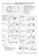
Bias set a dc output current up to 1.6 A without connecting input signal. 


You need an additional waveform generator which has to be connected to the 
input terminal. There is no AWG included within the driver! 


Step 

What to do 

Check 

Solder a dummy diode between LD+ and 
LD-. Alternatively make a short circuit 
there. 

See section “Test Load” 
 

Connect GND, VCC to power connector 
(power source disabled).  

VCC 24 V 
 

Connect waveform generator to input 
terminal (no pulse before enabling power 
supply). 

See all sections discussing input 
(connector #2). 
 

Enable the power source. 


Adjust scaling and bias. 

See potentiometer for scaling a 
bias. 

Feed a signal on the input terminal. For 
example 1 kHz sine wave with 1 V 
amplitude. 

Make sure not to overload the 
laser diode or the driver.  
Range of input signal 0 V .. 5 V. 

Monitor the current output. 

The current monitor measures a 
signal comparable with the input 
signal. Use an oscilloscope with a 
1 MEG ohm termination. Scale 165 
mV/A. 

Disable the input signal and turn off the 
power source.  
Remove the test diode or bypass and 
assemble the final laser diode. 


Turn the power supply for the VCC on 
again.  

VCC 24 V. 

10 

Feed a signal to the input terminal. 

Make sure not to overload the 
laser diode! 

Required Laser Diode Pinout 

The LDP-VRM 025-100 CA is designed for a direct connection to almost all kinds of laser 
diodes. The laser diode can be connected directly by a screw terminal. 
 

Summary of Contents for LDP-VRM 025-100 CA

Page 1: ...User Manual PicoLAS GmbH Burgstr 2 52146 Würselen Germany Phone 49 0 2405 64594 60 Fax 49 0 2405 64594 61 E mail info picolas de Web www picolas de Rev 1909 LDP VRM 025 100 CA ...

Page 2: ...t Overview 4 How to get started 5 Required Laser Diode Pinout 6 Power Driver Block Diagram 6 Description of the Connectors 6 Power Supply and absolute maximum Ratings 6 Input 7 Jumper 7 Current Monitor 7 Bias and scaling Potentiometers 7 Test Load 7 Power Dissipation 7 Mechanical Dimensions 7 ...

Page 3: ...GND and beyond VCC VCC Limit see table in section Power Supply 3 Peak output current 2 5 A Operating temperature range 0 C 60 C Best performance operating temperature range 10 C 35 C Storage temperature range 20 C 70 C Dos and Don ts Never ground any output connector Never use any grounded probes at the output Do not connect your oscilloscope to the output Driver and the probe will immediately be ...

Page 4: ...4 ...

Page 5: ...er source 5 Adjust scaling and bias See potentiometer for scaling a bias 6 Feed a signal on the input terminal For example 1 kHz sine wave with 1 V amplitude Make sure not to overload the laser diode or the driver Range of input signal 0 V 5 V 7 Monitor the current output The current monitor measures a signal comparable with the input signal Use an oscilloscope with a 1 MEG ohm termination Scale 1...

Page 6: ... Diagram Description of the Connectors Power Supply and absolute maximum Ratings Pin of conn 3 Allowed range Best performance Destroying limit 1 VCC laser supply 24 V 26 V 30 V 2 GND GND GND 3 Input terminal 0 V 5 V 5 3 V ...

Page 7: ...ent The scaling potentiometer varies with the scaling of the input signal Turn it right to increase the scale from 0 A V to 0 5 A V Test Load For the first test an appropriate test load may be assembled instead of the laser diode This test load can either be a short circuit or a Schottky diode like the ES3C Please connect the test load only between anode and cathode LD and LD and prevent shorts to...

Reviews: