background image

Philips Semiconductors

Product specification

PTN3501

Maintenance and control device

2001 Jan 17

12

POWER-UP TIMING

SYMBOL

PARAMETER

MAX.

UNIT

t

PUR

1

Power-up to Read Operation

1

ms

t

PUW

1

Power-up to Write Operation

5

ms

NOTE:
1. t

PUR

 and t

PUW

 are the delays required from the time V

CC

 is stable until the specified operation can be initiated. These parameters are

guaranteed by design.

WRITE CYCLE LIMITS

SYMBOL

PARAMETER

MIN.

TYP.

 (5)

MAX.

UNIT

t

WR

1

Write Cycle Time

5

10

ms

NOTE:
1. t

WR

 is the maximum time that the device requires to perform the internal write operation.

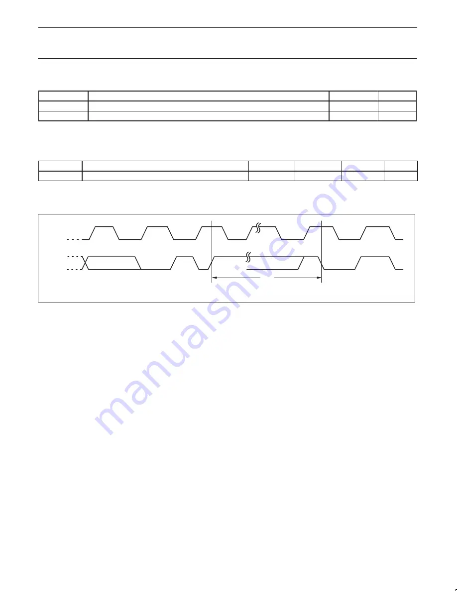
Write Cycle Timing

SCL

SDA

8th Bit

Word n

ACK

Stop
Condition

Start
Condition

MEMORY

ADDRESS

t

WR

SW00560

Figure 20.  

Summary of Contents for PTN3501

Page 1: ... PTN3501 Maintenance and control device Product specification Supersedes data of 2000 Nov 22 2001 Jan 17 INTEGRATED CIRCUITS ...

Page 2: ...s allowing up to 64 devices to share the common two wire I2C software protocol serial data bus The PTN3501 supports live insertion to facilitate usage in removable cards on backplane systems The PTN3501 is an alternative to the functionally similar PTN3500 for systems where a high number of devices are required to share the same I2C bus without need for an additional I2C bus I O expander PIN CONFI...

Page 3: ...e 3 Start and stop conditions Both data and clock lines remain HIGH when the bus is not busy A HIGH to LOW transition of the data line while the clock is HIGH is defined as the start condition S A LOW to HIGH transition of the data line while the clock is HIGH is defined as the stop condition P see Figure 4 System configuration A device generating a message is a transmitter a device receiving is t...

Page 4: ... to pull down the SDA line during the acknowledge clock pulse so that the SDA line is stable LOW during the HIGH period of the acknowledge related clock pulse set up and hold times must be taken into account A master receiver must signal an end of data to the transmitter by not generating an acknowledge on the last byte that has been clocked out of the slave In this event the transmitter must leav...

Page 5: ... as an input or output Input I O data is transferred from the port to the microcontroller by the READ mode See Figure 10 Output data is transmitted to the port by the I O WRITE mode see Figure 9 S 0 A5 A4 A3 A2 A1 A0 0 A DATA 1 A DATA 2 A SDA SCL tpv 1 2 3 4 5 6 7 8 tpv DATA 2 VALID DATA 1 VALID SW00649 ACKNOWLEDGE FROM SLAVE R W START CONDITION ACKNOWLEDGE FROM SLAVE ACKNOWLEDGE FROM SLAVE SLAVE ...

Page 6: ...ignal In the WRITE mode at the acknowledge bit after the HIGH to LOW transition of the SCL signal Returning of the port data to its original setting A second port state change will require an SCL rising clock edge to be captured as an INT event Interrupts which occur during the acknowledge clock pulse may be lost or very short due to the resetting of the interrupt during this pulse Each change of ...

Page 7: ... and are switched off by the negative edge of SCL The I Os should be HIGH before being used as inputs S 0 A2 A1 A0 0 A A A SDA SCL 1 2 3 4 5 6 7 8 SW00789 ACKNOWLEDGE FROM SLAVE R W START CONDITION ACKNOWLEDGE FROM SLAVE SLAVE ADDRESS PTN3501 DATA TO PORT DATA TO PORT 1 P3 0 P3 P P3 OUTPUT VOLTAGE P3 PULL UP OUTPUT CURRENT IOHt IOH A5 A4 A3 Figure 13 Transient pull up current IOHt while P3 changes...

Page 8: ...he quasi bidirectional I Os are allowed during the internal write cycle Page Write see Figure 15 A page write is initiated in the same way as the byte write if after sending the first word of data the stop condition is not received the PTN3501 considers subsequent words as data After each data word the PTN3501 responds with an acknowledge and the four least significant bits of the memory address f...

Page 9: ...and use the next eight clock cycles to transmit the data contained in the addressed location The master ceases the transmission by issuing the stop condition after the eighth bit omitting the ninth clock cycle acknowledge Sequential Read see Figure 18 The PTN3501 sequential read is an extension of either the current address read or random read If the master doesn t issue a stop condition after it ...

Page 10: ... MAX UNIT Supply VDD Supply Voltage 2 5 3 3 3 6 V IDDQ Standby Current A0 thru A5 WC HIGH 60 µA IDD1 Supply Current Read 1 mA IDD2 Supply Current Write 2 mA VPOR Power on Reset Voltage 2 4 V Input SCL input output SDA VIL Input LOW voltage 0 5 0 3 VDD V VIH Input HIGH voltage 0 7 VDD 5 5 V IOL Output LOW current VOL 0 4 V 3 mA IL Input leakage current VI VDD or VSS 1 1 µA CI Input capacitance VI V...

Page 11: ...SDA rise time 0 3 µs tf SCL and SDA fall time 0 3 µs tSU DAT data set up time 250 ns tHD DAT data hold time 0 ns tVD DAT SCL LOW to data out valid 1 0 µs tSU STO STOP condition set up time 0 6 µs NOTE 1 All the timing values are valid within the operating supply voltage and ambient temperature range and refer to VIL and VIH with an input voltage swing of VSS to VDD handbook full pagewidth SCL SDA ...

Page 12: ...UW are the delays required from the time VCC is stable until the specified operation can be initiated These parameters are guaranteed by design WRITE CYCLE LIMITS SYMBOL PARAMETER MIN TYP 5 MAX UNIT tWR 1 Write Cycle Time 5 10 ms NOTE 1 tWR is the maximum time that the device requires to perform the internal write operation Write Cycle Timing SCL SDA 8th Bit Word n ACK Stop Condition Start Conditi...

Page 13: ...conduction by heated belt Dwell times vary between 50 and 300 seconds depending on heating method Typical reflow temperatures range from 215 to 250 C Preheating is necessary to dry the paste and evaporate the binding agent Preheating duration 45 minutes at 45 C Wave soldering Wave soldering is not recommended for SSOP packages This is because of the likelihood of solder bridging due to closely spa...

Page 14: ...Philips Semiconductors Product specification PTN3501 Maintenance and control device 2001 Jan 17 14 TSSOP20 plastic thin shrink small outline package 20 leads body width 4 4 mm SOT360 1 ...

Page 15: ...make changes Philips Semiconductors reserves the right to make changes without notice in the products including circuits standard cells and or software described or contained herein in order to improve design and or performance Philips Semiconductors assumes no responsibility or liability for the use of any of these products conveys no license or title under any patent copyright or mask work right...

Reviews: