background image

Service Modes, Error Codes, and Fault Finding

EN 8

LGE PDP

5.

5.

Service Modes, Error Codes, and Fault Finding

Index of this chapter:
5.1  Quick Module Check PDP42V7*
5.2  Detailed Module Check PDP42V7*
5.3  Detailed PSU Check PDP42V7*

5.1

Quick Module Check PDP42V7*

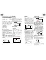
Figure 5-1 Logical judgement

Figure 5-2 Quick check

What kind of defect? 

Horizontal defect?

Vertical defect?

Please follow the “No display” trouble shooting way (see figure below).  

No display?

Dark display?

Please follow the “Dark display” trouble shooting way (see figure below).

Bar defect appeared?

Please follow “Bar defect” trouble shooting
way (see figure below).

Line defect

Please follow the “Line defect” trouble shooting way (see figure below).

Mis–discharge

on screen?

Please follow the “Mis-discharge” trouble shooting way (see figure below).

F_15590_064.eps

050705

Trouble Shooting

Horizontal defect?

Vertical defect?

Mis –discharge

on screen?

No display?

Check model No. of module, all connectors and cables.

Check panel appearance

Check PSU output (Va,Vs,5v)

Check Y, Z B/D Input 
voltage

Replace Ctrl B/D

Replace Y, Z B/D

Dark display ?

Check IPM of Y SUS ,Z B/D

Replace YDR B/D

Check all cables and connectors

Replace Ctrl B/D

Check panel appearance

Check TCP

Replace X B/D

Replace Ctrl B/D

Check FPC

Replace YDR B/D

Replace YSUS B/D

Replace Ctrl B/D

Replace YDR B/D

Replace YSUS B/D

F_15590_063.eps

050705

Summary of Contents for PDP42V7 series

Page 1: ...ying or otherwise without the prior permission of Philips Colour television Module LGE PDP Repair Manual PDP42V7 Contents Page 1 Technical Specifications Connections and Chassis Overview 2 2 Safety Instructions Warnings and Notes 5 3 Directions for Use 5 4 Mechanical Instructions 6 5 Service Modes Error Codes and Fault Finding 8 6 Block Diagrams Test Point Overviews and Waveforms 24 7 Circuit Diag...

Page 2: ...at centre Contrast Ratio Typical 10000 1 Dark room 1 10 white window white window pattern at centre Power Consumption Typical 200 W Full White 1 Lifetime Over 60 000 Hrs Initial brightness 1 2 Note 1 It can increase to 300 W depending on input image 1 1 2 Definitions Figure 1 1 Definition of module position Figure 1 2 Identification label 1 Model name 2 Bar code Code 128 contains the manufacture n...

Page 3: ...SUS board 5V P9 CTRL board Control signal No LGE Part No Description A 6631Q39032A Cable assy 10p PSU Y SUS B 6631Q39033A Cable assy 8p PSU Z SUS C 6631Q39034A Cable assy 4p PSU Y SUS No Input voltage signal CN806 Vs 187 V CN807 Vs 187 V Va 65 V 5 V CN805 5V CN1308 AC 220 V 1M02 Vsnd 18 V Vsnd 18 V 1M46 8V6 8 6 V 12V 12 V 5V2 5 2 V Vtun 50 V 1M03 5V_sw 5 2 V No LGE Part No Description of board ass...

Page 4: ...ons Connections and Chassis Overview EN 4 LGE PDP 1 1 1 4 Chassis Overview Figure 1 8 PWB location CONTROL B D Y DRIVE BOTTOM Y SUS F_15590_040 eps 170605 B D Y DRIVE TOP X LEFT B D X RIGHT B D Z SUS B D PSU VOLTAGE IPM TCP ...

Page 5: ...ing components or circuit boards in order to repair be sure to fix a lead line to the connector before soldering 14 If inserting high power resistors metal oxide film resistor or metal film resistor in order to repair insert it 10 mm away from a board 15 During repairs high voltage or high temperature components must be put away from a lead line 16 This is a cold chassis but you better use an isol...

Page 6: ...rview PDP42V7 Figure 4 1 Cable dressing Figure 4 2 Label location F_15590_060 eps 200605 F_15590_000 eps 010705 F_15590_110 eps 070705 CTRL B D Y SUS Y DRV TOP Y DRV BTM X L B D X R B D Serial No Position an Information Board P No Board Name Serial No of Assembly Information of module ...

Page 7: ... Mark ྟ Safety Approval Mark ྠ Safety Approval No 3 Voltage Label Model Name Operational Voltage 195 120 115 N A N A 230W 190V 5V 7 2 5 7 0 F_15590_112 eps 080705 4 Serial No for Frame Ass y ྙ ྙ Serial No of Frame Ass y Serial No of Frame Ass y for Philips are 3315Q E037B 3315Q E037C and 3315Q E037F 5 Manufacture Serial No Label of Module ྟ 2004 1 410K342V7001266 AKLGG21 7 ྞ ྜྷ ྜ ྛ ྚ ྙ 2 5 7 0 ྙ Mo...

Page 8: ... trouble shooting way see figure below Line defect Please follow the Line defect trouble shooting way see figure below Mis discharge on screen Please follow the Mis discharge trouble shooting way see figure below F_15590_064 eps 050705 Trouble Shooting Horizontal defect Vertical defect Mis discharge on screen No display Check model No of module all connectors and cables Check panel appearance Chec...

Page 9: ...e 5 3 Control Y SUS board Figure 5 4 Control Z SUS board Figure 5 5 Control X board Figure 5 6 Signal input LVDS Exhaust Tip Check the Exhausting Tip for cracks with the naked eye to check the vacuum state If there is a problem replace the PDP module by a new one In case of vacuum breakdown the module makes a shaking noise because of inside gas ventilation There may be a small crack which cannot b...

Page 10: ...e boards when a short occurs on circuits of the PDP module or when a power problem occurs If there is no power even after replacing the PSU find out where the short occurred In case of a PSU protection the red LED will be on and an error code will be displayed via the green blinking LED see also paragraph Detailed PSU Trouble Shooting further on In case of a PSU protection switch the service switc...

Page 11: ...tages Vsetup Vy and Vsc 3 Check diode between GND and Y SUS output 4 Check whether output voltages agree with voltages on the label Figure 5 10 Y SUS board output diode check Figure 5 11 Y SUS b d trouble shooting F_15590_072 eps 060705 3 3 V 5 V 1 8 V LED Input voltage OSC X1 Probe touching point Check FET Check oscillating state Be careful with physical shock DMM GND F_15590_074 eps 290605 Norma...
Page 12: ...t section Connector Check the TCP connector and cables If not connected well it will result in a bar defect and abnormal display behaviour Figure 5 14 Connector check 1 Figure 5 15 Connector check 2 Checking TCP Confirm whether the TCP was torn or chopping Figure 5 16 TCP torn Figure 5 17 TCP IC broken F_15590_075 eps 070705 Va FUSE Vs FUSE 5V FUSE F_15590_077 eps 060705 Normal diode value 0 4 for...

Page 13: ... of Control board defect The MCM cannot be replaced separately So replace the Control board Figure 5 20 Evenly repeated lines 5 1 4 Bar Defect Horizontal Most horizontal defects can be repaired In case of adherence part of the film and rear panel electrode or panel electrode open short replace the PDP panel Connector If the connector on Y board and Z board are not plugged in well it can result in ...

Page 14: ...S or Z board Check these boards when mis discharge occurs Figure 5 26 Mis discharge Checking Order 1 Check Y and Z SUS signal cable 2 Check if Y DRV IC is defective 3 Check Y SUS board voltages Vy Vscw 4 Check if Y and or Z SUS IPM are defective see paragraph How to Check IPM below 5 Replace Control board How to Check IPM Forward direction Measure between GND and Sus out Sus out and Vs When each t...

Page 15: ...d Z boards with an oscilloscope 200 MHz and find the trouble board by comparing the output wave with below figure Measure point for Y board Bead B39 Measure point for Z board Bead B28 Measure point for X board P3 6 Check the SCAN Y side IC 7 Check the DATA X side TCP IC 8 Replace the CTRL board 9 Check if the fuse of Y and or Z board is open and replace when open 10 Check the input voltage Vcc 5 V...

Page 16: ...ata TCPs can be shown Figure 5 32 Screen display Vertical parts missing How to examine Data TCP IC Change 1 Va Power into CATHOD 2 GND into ANODE and then examine the diode in forward or reverse direction Examine with the naked eye traces of blown ICs 3 or others Figure 5 33 Data TCP IC examination Unusual Pattern on Display 1 In case of generating unusual pattern of Data TCP IC unit as shown in b...

Page 17: ... Flash at Special Colour Replace the CTRL board Figure 5 42 Screen display Vertical lines with regular gap Data Copy into Vertical Direction Replace the Y DRV board or Y board Figure 5 43 Screen display Data copy in vertical direction One or Several Vertical Line s on the Screen 1 It may be caused by Open or short on DATA TCP FPC attached panel Defect on DATA TCP attached panel 2 Replace Module Un...

Page 18: ... When the internal Sustain_IGBT or ER_FET of Y IPM IC15 or Z IPM IC2 is damaged VS fuse is open and there will be no picture Test Point B32 GND Y board B28 GND Z board Wave format B32 Y board or B28 Z board has no output wave Measure position Sustain section B32 wave of Y board and B28 wave of Z board full white pattern Figure 5 47 IPM normal output Pass_Top FET Y board HS2 When the Pass_Top FET i...

Page 19: ...f GND Y DRV board output Wave format As shown in figure Y DRV board Top and Bottom cable damaged 4 Overlap of two horizontal lines on the screen in case of shorted SCAN IC output Test Point ICT measurement of GND Y DRV board output Wave format As shown in figures SCAN IC shorted output and SCAN IC normal output Measurement point SCAN section output ICT of Y DRV board full white pattern Figure 5 52...

Page 20: ...P of GND TCP Wave format Output wave is not generated Figure 5 56 COF IC output defective Figure 5 57 TCP normal output Crystal CTRL board X1 1 When a crystal is damaged the screen is not shown Test Point Measuring 3 pin of GND Crystal CTRL board X1 Wave format Output wave is not generated 2 In case of unusual start up of the crystal the screen may blink Wave format As shown in figure below Measur...

Page 21: ...E PFC FET PFC FET STBY TRANS CN 8 0 6 CN 8 0 6 PFC COIL CN 8 0 7 CN 8 0 7 BRIDGE DIODE 1 M 0 2 1 M 0 2 CN 8 0 5 CN 8 0 5 MAIN CAP MAIN CAP 1M03 1 1M03 1 1M46 1 1M46 1 1 Bridge Bridge FET FET DIODE DIODE DIODE DIODE F_15590_097 eps 040705 To Audio To Philips SSB F_15590_098 eps 040705 F_15590_099 eps 040705 F_15590_100 eps 040705 Check LED s on Power Supply Only Green LED is on Set is in Standby Re...

Page 22: ... 8V6 circuit protection Figure 5 72 18V circuit protection Figure 5 73 PFC circuit protection F_15590_101 eps 040705 slkG j G vjwG v Gj Gw G v wG v G Gw G j G G G G Q G GaGslkGvuVvmmG G G GYWW G slkGvuG slkGvmmG slkGvu slkGvmm F_15590_102 eps 040705 slkG j G vjwG v Gj Gw G v wG v G Gw G YG G G slkGvuG slkGvmmG XU z _W y G XU z _W y G slkGvu slkGvmm F_15590_103 eps 040705 slkG j G vjwG v Gj Gw G v ...

Page 23: ... Only partial picture Unstabel picture Flickering flashing picture Lines across down image Inactive row s Inactive column s Missing colour s Other Pixel Defect s Dark dots Bright dots Qty of dots Mark Defect s Following defect symptoms are out of warranty R I A P E R L E N A P Symptoms Out of warranty Broken glass Scratch es on display Number of dark bright pixels within spec Burn in only for Plas...

Page 24: ...Block Diagrams Test Point Overviews and Waveforms EN 24 LGE PDP 6 6 Block Diagrams Test Point Overviews and Waveforms Not applicable ...

Page 25: ...Circuit Diagrams and PWB Layouts EN 25 LGE PDP 7 7 Circuit Diagrams and PWB Layouts Not applicable ...

Page 26: ...ram 2 Turn on the measuring instruments with Caution of Fig Measuring equipment connection diagram 3 Connect the oscilloscope probe to B39 Bead of Y board bottom and GND 4 Turn the VR1 on the Y board and make the A waveform according to Fig Y Z set up waveform to be 10 2 µs Vset down Alignment Adjusting Vset down voltage wave form 1 Turn the VR2 on the YSUS board and make the B waveform according ...

Page 27: ...ent step 1 Figure 8 4 Connect Mains Vs alignment step 2 Figure 8 5 Vs measure and alignment point step 3 4 8 2 4 Internal Test Patterns The CTRL board is capable of generating it s own video test patterns There are two possibilities both based on R406 and R407 R406 is open and R407 is fitted standard setting the test pattern is a full black screen very low light output R406 is fitted and R407 is o...

Page 28: ...upplies this waveform to TCP data Figure 9 1 X boards 9 1 2 Dismantling 1 Remove connections between the boards Figure 9 2 Between CONTROL board and X board 1 Lift up lock as indicated by the arrows handle with care as this part is easy to break 2 Pull TCP as indicated handle with care as the TCP film part is easy to damage Figure 9 3 TCP Separating 9 2 Z Sustain Board 9 2 1 Purpose To make the SU...

Page 29: ...n GND and Vpp only in SCAN period Note In case of 42 V7 used DRIVER SCAN ICs are in total of 8 EA TOP BOTTOM each 4 EA Figure 9 6 Y Drive board 9 4 Y Sustain Board 9 4 1 Purpose Generates SUSTAIN RESET and Vsc SCAN voltages and supplies them to the Y DRIVE board Figure 9 7 Y Sustain board 9 4 2 Main Components IPM diode electrolytic capacitor and FET 9 5 Control Board 9 5 1 Purpose Creates signal ...

Page 30: ...d Circuit 9 8 FFC Flat Flexible Cable 9 8 1 Purpose For connecting LOGIC signals between boards There are two types 0 5 mm pitch 50 pin type 0 5 mm pitch 60 pin type Figure 9 12 Flat Flexible Cable 9 9 TCP Tape Carrier Package 9 9 1 Purpose To supply a waveform which is made by the X board to the PDP and to select an output pin that is controlled by TCP when on or off 192 output pins per IC TCP is...

Page 31: ...ternating Current B D Board CLK Clock signal CTRL Control board DC Direct Current FET Field Effect Transistor FPC Flexible Printed Circuit I O Input Output IC Integrated Circuit IPM Intelligent Power Module LED Light Emitting Diode LGE Lucky Goldstar Electronics supplier MCM Multi Chip Module PCB Printed Circuit Board same as PWB PDP Plasma Display Panel PFC Power Factor Corrector circuit PSU Powe...

Page 32: ... m G XWhSGZWW ozX o Gz Oml P U QZWQY QXU Gz iVk XW XW mzX XWhSGXY mzY mYWsjZW YU Who G Y W OG G P U Who G Y W OG G P S S S S S S S S S S S S S S Z WX hGOGGGGGP S S X nl Gw X XW WW hGGOGGGGGP msX nl Gw OGGP W o ZZU G S S ozY o Gz _U QZWQYXU QXUW S S Gz iVk z Y W X W Y W X W j SXWSXXSXYSXZ YWhVZWW zopuklunlu zmYWsjZW kX mzX XW XW mzZ XWhSGXY m G XWhSGZWW mYWsjZW mYWsjZW YU Who G Y W OG G P U Who G Y...

Page 33: ...Revision List EN 33 LGE PDP 11 11 Revision List Manual xxxx xxx xxxx 0 First release ...

Page 34: ...Revision List EN 34 LGE PDP 11 ...

Reviews: