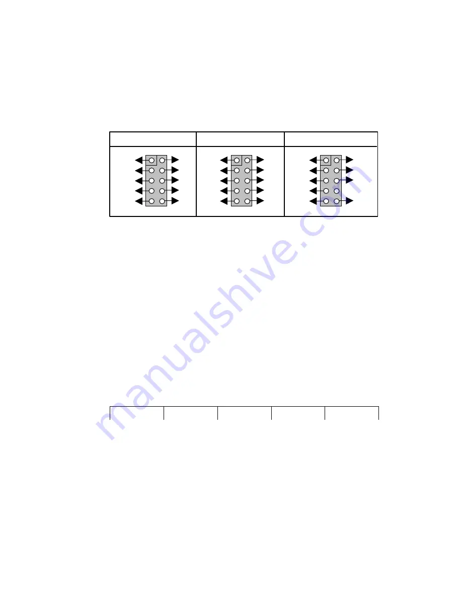
ANALOG INPUT (J3) header consists of pins that can be used as analog inputs
or digital inputs/outputs. A7 pin can also be used as Counter 1.
DIGITAL I/O (J4) header consists of pins that can be used as digital
inputs/outputs. DIO7 pin can also be used as Counter 0.
GPIO & I2C (J10) header consists of pins that can be used as digital
inputs/outputs as well as SDA and SCL pins for I
2
C.
Specification and characteristics of each pin can be seen in the datasheet.
3.
INTERFACE
PC-LINK USB SMART I/O has a USB interface that will be recognized and
accessible by computer as UART COM port (virtual).
3.1.
UART Interface
UART communication parameters are as follows:
•
110 – 256000 bps
•
8 data bit
•
1 stop bit
•
no parity bit
•
no flow control
Each data packet sent by host begins with initial byte that is followed with 1
byte sum of command byte+data, 1 byte command code, n byte parameter (if
needed) and ends with 1 byte LRC.
Start Byte
Byte Count
Command
Parameter
LRC
Start Byte always have 0x58 ($58) hexadecimal or 88 decimal value.
Byte Count is the sum of Command and Parameter byte (excluding Start Byte,
Byte Count, and LRC).
LRC is an error checking byte by summing all bytes, from Start Byte to the last
Parameter. Only LSB will be taken from the sum results and two's complement
will be performed.
PC-LINK USB SMART I/O has a timeout feature for packet reception from host.
If there is no received data in ± 1 second, the next data will be treated as a
new data packet and module will wait for Start Byte.
If timeout occurs in the middle of the packet, then the packet will be ignored.
For commands that ask for data, the format of replied data packet from the
module will be the same as the format of data packet from the host
.
7
AGND
A0
A2
A4
A6
VCC
A1
A3
A5
A7
2
1
10
9
ANALOG INPUT (J3)
DIGITAL I/O (J4)
PGND
DIO0
DIO2
DIO4
DIO6
VCC
DIO1
DIO3
DIO5
DIO7
2
1
10
9
PGND
GPIO0
GPIO2
GPIO4
SDA
VCC
GPIO1
GPIO3
SCL
2
1
10
9
GPIO & I2C (J10)


