background image

Set remains closed!

N

Y

Play a CD 

for at least 10 minutes

Y

playability

ok ?

N

playability

ok ?

add Info for customer

"SET OK"

check playability

N

Y

playability

ok ?

check playability

check playability

return set

Customer complaint

"CD related problem"

"fast" lens cleaning

1

2

3

For flap loaders (= access to CD drive possible)
cleaning method 

4

 is recommended

INSTRUCTIONS ON CD PLAYABILITY

2 - 1

Exchange CDM

1

-

4

For description - see following pages

Summary of Contents for MCD107

Page 1: ...means electronic mechanical photocopying or otherwise without the prior permission of Philips CONTENTS Technical specification 1 2 Service measurement setup 1 3 Service aids 1 4 Instructions on CD playability 2 1 2 2 Disassembly diagram 5 1 Block diagram 3 1 Wiring diagram 4 1 Main board Circuit diagram 6 1 6 2 Layout diagram 6 3 6 4 DVD board Circuit diagram 7 1 7 5 Layout diagram 7 6 Exploded vi...

Page 2: ...0 5 V RMS 20 kohm Disc Laser type Semiconductor Disc diameter 12 cm 8 cm Video decoding MPEG 2 MPEG 1 Video DAC 10 bits Signal system PAL NTSC Video format 4 3 16 9 Video S N 56 dB minimum Composite video output 1 0 Vp p 75 ohm S Video output Y 1 0 Vp p 75 ohm C 0 286 Vp p 75 ohm Audio DAC 24 bits 96 kHz Total harmonic distortion 1 Frequency response 4 Hz 20 kHz 44 1kHz 4 Hz 22 kHz 48 kHz 4 Hz 44 ...

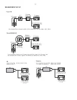
Page 3: ...15kHz e g 7122 707 48001 LF Voltmeter e g PM2534 DUT S N and distortion meter e g Sound Technology ST1700B Frame aerial e g 7122 707 89001 Tuner AM MW LW To avoid atmospheric interference all AM measurements have to be carried out in a Faraday s cage Use a bandpass filter or at least a high pass filter with 250Hz to eliminate hum 50Hz 100Hz RF Generator e g PM5326 Ri 50 Bandpass 250Hz 15kHz e g 71...

Page 4: ...ng make sure that you are connected with the same potential as the mass of the set via a wrist wrap with resistance Keep components and tools also at this potential ESD CLASS 1 LASER PRODUCT GB Safety regulations require that the set be restored to its original condition and that parts which are identical with those specified be used Safety components are marked by the symbol Lead free ...

Page 5: ...T OK check playability N Y playability ok check playability check playability return set Customer complaint CD related problem fast lens cleaning 1 2 3 For flap loaders access to CD drive possible cleaning method 4 is recommended INSTRUCTIONS ON CD PLAYABILITY 2 1 Exchange CDM 1 4 For description see following pages ...

Page 6: ...viously caused by a scratched dirty or copy protected CD In case problems remain the customer is requested to contact the workshop directly The lens cleaning method 3 should be mentioned in the addendum sheet The final wording in national language as well as the printing is under responsibility of the Regional Service Organizations 4 LIQUID LENS CLEANING Because the material of the lens is synthet...

Page 7: ...3 DVD DATA 4 DVD IR MACHANISM SONY KHM313 KEY I2C UE2314 CHANNEL SEL DSC VOLUME CONTROL DVD AUDIO_OUT DVD AUDIO_IN AUX IN AUDIO_OUT IN K P S R K P S L L SPK OUT R SPK OUT TFA9842BJ POWER AMP DC POWER SUPPLY TRANSFORM KEY CONTROL SDRAM HY57V641620ETP 7 FLASH NJM4558 1 F 2 F 3 T 4 T DVD BOARD MOTOR DRIVER AM5888S DVD SUPPLY AUX USB AC IN1 27MHz DISPLAY BOARD MAIN BOARD MAIN BOARD ...

Page 8: ...WIRING DIAGRAM 4 1 4 1 CN404 CN402 CN401 CN405 CN901 CN963 CN961 CN910 CN950 CN901 CN101 CN104 CN100 CN5 CN102 CN103 FM ANT DISPLAY PCB TRANSFORMER EI57 MAIN PCB DVD PCB CN3 JK903 JK902 JK901 ...

Page 9: ...6 screws C as indicated to loosen the Bottom Cabinet Dismantling of the Bottom Cabinet Dismantling of the Front Cabinet and PCB Board D 1 Remove 2 screws D as indicated to loosen the Front Cabinet 2 Remove 9 screws E as indicated to loosen the Front Board 3 Remove 2 screws F as indicated to loosen the Main Board E B F ...

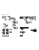
Page 10: ...001 R919 1K 1 6W C936 0 47UF D901 3V3 D903 BAS316 D958 1N4001 R933 470K R996 150R 1 2W D961 1N4001 C937 0 47UF R975 220K R922 10K Q932 3904 R979 47K R927 15K D932 BAS316 R949 15K R950 15K R918 100R M C924 3 3U 50V R980 22K C940 470U 25V R995 150R 1 2W C900 NC D580 SS14 L580 27uH R605 10K Q583 3904 R616 10K 1 BS 2 IN 3 SW 4 GND 5 FB 6 COMP 7 EN 8 NC U003 MP1583 C580 223 Q580 3904 R618 10K R600 30K ...

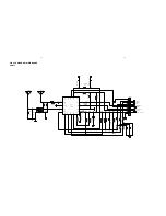
Page 11: ...6V C305 0 022UF 1 2 3 4 5 6 7 8 9 10 JCN303 1 FM ANT C301 22PF 1 AM ANT C307 NC R30110K C3020 1UF R30710K R30510K R30410K X301 32 768KHZ C303 22PF C304 22PF R311 NC R316 NC C308 NC 1 3 6 4 2 5 T301 L302 L301 L304 L303 D303 NC D304 NC D302 BAS316 D301 BAS316 R308 0R L306 FB L307 FB L308 FB R322 1K R321 1K R320 1K C320 NC C321 100P C322 100P SD CLK RES SD DATA TUNER ROUT TUNER LOUT OSC RES TUNER VCC...

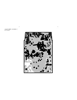
Page 12: ...6 3 6 3L LAYOUT DIAGRAM MAIN BOARD TOP SIDE ...

Page 13: ...6 4 6 4 LAYOUT DIAGRAM MAIN BOARD BOTTOM SIDE ...

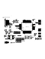
Page 14: ...3 CON9 1 2 3 4 5 6 7 8 9 Q12 2SS8550D EBC 1 5A 1W U3 MP1853 SOP8 1 2 3 4 5 6 7 8 BS Vin Vsw GND FB Comp EN NC R188 11K 1 L8 FB C91 0 1uF R184 10K R187 20K 1 0 1uF BC16 L12 27uH 1 5A EC16 220uF 16V R186 10K C88 0 022uF R185 10K L27 FB C90 3 9N EC17 10uF 16V H1 1 2 3 4 5 6 7 8 9 1 2 3 4 5 6 7 8 9 D11 SS14 SMD R1 2 2 H3 1 2 3 4 5 6 7 8 9 1 2 3 4 5 6 7 8 9 L11 FB EC6 100uF 16V H4 1 2 3 4 5 6 7 8 9 1 2...

Page 15: ... RF3 3V GND RFGND TP8 EC5 47uF 16V TP9 TP11 TP12 R117 100K R192 10K R32 5 1 R78 1K R112 100K R191 10K R190 10K R189 10K L15 FB EC3 47uF 16V 0 1uF BC3 EC19 1uF 16V R115 NC 0 R111 10K 0 1uF BC28 0 1uF BC2 0 1uF BC6 R127 2 2K 0 1uF BC25 0 1uF BC12 EC9 47uF 16V R116 10K 0 1uF BC26 0 1uF BC29 0 1uF BC34 0 1uF BC32 EC10 10uF 16V 0 1uF BC14 0 1uF BC35 0 1uF BC15 0 01uF BC17 TP7 Reset EC8 47uF 16V R42 4 7...

Page 16: ...GND SPI_VCC3 GND SPI_VCC3 SPI_VCC3 SPI_VCC3 GND GND R194 330 U10 SDRAM 1Mx16x4 23 24 25 26 29 30 31 32 33 34 17 18 15 16 19 37 38 39 2 4 5 7 8 10 11 13 42 44 45 47 48 50 51 53 36 20 1 27 28 41 22 40 3 9 43 49 6 12 46 52 35 21 54 14 A0 A1 A2 A3 A4 A5 A6 A7 A8 A9 CAS RAS LDQM WE CS CKE CLK UDQM D0 D1 D2 D3 D4 D5 D6 D7 D8 D9 D10 D11 D12 D13 D14 D15 NC BA0 VDD VDD VSS VSS A10 AP NC RFU VDDq VDDq VDDq ...

Page 17: ... U B U B Y S O _ Y G Y G V_COMP V_FSADJ CVB1_O B U_O G Y_O SY R V_O SC G Y R V B U CVB1 CVB1 G Y B U R V V_FSADJ V_COMP CVB1_O 2 G Y_O 2 R V_O 2 B U_O 2 TV_DAC0 3 TV_DAC1 3 TV_DAC2 3 TV_DAC3 3 V_FSADJ 3 V_COMP 3 VVCC3 GND P 5V GND P 5V GND P 5V GND P 5V GND GND GND GND GND D5 BAV99 EC20 10uF 16V D6 BAV99 D7 BAV99 D8 BAV99 100pF C74 100pF C73 L34 1uH 10pF C68 100pF C12 10pF C21 100pF C19 L10 1uH R5...

Page 18: ...200pF C86 Q24 2N3904 1200pF C78 10uF 10V C82 R135 9 1K 10uF 10V C77 EC21 100uF 16V C87 1uF R133 33K R132 33K R131 10 R128 470 R21 150 Q23 2N3906 10pF C11 0 1uF C7 R106 0 R109 2 2K R105 470 ZD1 Zener 5V1 DIP Q16 2N3906 EC15 470uF 16V R150 470 10uF 10V C3 10uF 10V C14 10uF 10V C15 10uF 10V C4 R23 4 7K R13 470 47pF C1 R11 100K 1200pF C9 120pF C5 Q2 2N3904 U2A NJM4558 3 2 1 8 4 R30 9 1K R20 24K R9 100...

Page 19: ...7 6 7 6 LAYOUT DIAGRAM DVD BOARD ...

Page 20: ...403 ECO_LED R419 1K R430 4K7 L403 F B L402 F B L401 F B C402 100P C403 100P C401 100P C406 100U 16 C407 104 Q402 8050 R425 47K L407 F B L406 F B C414 220P C415 220P L422 F B L421 F B R438 10R C433 100U 16 C425 220P C424 220P R460 15K R461 15K R437 47K R436 47K R435 47K R434 47K R424 1K C434 N C C435 N C C436 N C C437 N C C438 N C C439 N C C440 N C C441 N C C442 N C C443 N C C444 N C C445 N C C446 ...

Page 21: ...8 2 8 2 LAYOUT DIAGRAM FRONT BOARD TOP SIDE ...

Page 22: ...8 3 8 3 LAYOUT DIAGRAM FRONT BOARD BOTTOM SIDE ...

Page 23: ...SET EXPLODED VIEW DIAGRAM 9 1 9 1 ...

Page 24: ...6 TRIM RING J003 996510012092 24P FFC 0 5mm L 140mm J002 996510029287 AC SOCKET R 201A B00 BLACK J004 996510029017 17P FFC 1mm L 120mm J007 996510029034 AC CORD VDE APP 2M only for 51 J007 994000003633 AC CORD SET 10A 1 83M VDE APP only for 98 S001 994000004376 SWITCH SL14 22AH 5AN S002 994000002354 CD DOOR SWITCH DLS 02 W 1 T001 996510029015 TRANSFORMER EI57 230V only for 51 T001 996510029015 TRA...

Page 25: ...4000001965 LED LAMP 3MM RED D415 994000005385 LED LAMP WHITE D416 994000005385 LED LAMP WHITE IC402 996510020822 IC AT24C02BN IC403 994000002839 IC LM1117S 3 3 IC406 996510029027 IC GY680 LQFP44 1010 OTP JK401 996510001316 USB SOCKET 4P JK402 994000001244 V PHONE JACK 3 5MM JK402 994000001244 V PHONE JACK 3 5MM JK403 994000001244 V PHONE JACK 3 5MM LCD1 996510029074 LCD DISPLAY SDM8A5788A HPTNN P4...

Page 26: ...S MP1583 SOP 8 U2 996500039809 IC YD4558 U200 996510026072 IC UTC7812 TO 220 1 5A U3 996500039809 IC YD4558 U4 996510026057 IC D5888S HSOP28 U6 996510026054 ICSPHE8202TS HL11M LQFP128PIN U8 996510026053 IC EN25T80 FLASH OTP SOP 8 X1 996510009448 CRYSTAL27MHzHC49 US30PF 20PPM TUNER BOARD ASSEMBLY only for 98 IC301 996510018861 IC SI4702 Note Only these parts mentioned in the list are normal service...

Reviews: