


TROUBLESHOOTING
Tr
oub
leshooting
W
ARNING
Under no circumstances should you tr
y to r
epair the system your
self,
as this will in
validate the
w
arr
anty
. Do not open the system as ther
e is a risk of electric shock.
If a fault occur
s,
fir
st check the points listed belo
w befor
e taking the system for repair
. If you
ar
e unable to r
e
medy a pr
oblem b
y
follo
wing these hints
, consult your dealer or ser
vice center
.
Pr
ob
lem
Solution
CD OPERA
TION
“
NO DISC
”
is displa
y
ed.
–
Inser
t a disc
.
–
Check if the disc is inser
ted upside down.
–W
ait until the moisture condensation at the lens
has cleared.
–
Replace or clean the disc
, see “Maintenance”.
–
Use a f
inalised CD-R
W or CD-R.
No pictur
e on
TV scr
een.
–
Connect the cable betw
en the system and
TV
.
No colour on
TV
.
–
Change the system to the respective P
AL or
NTSC setting.
Cannot adjust the
TV system to
–
Remo
ve the MP-3 CD from disc tr
ay
PA
L
or NTSC
.
Maintenance
Cleaning the Cabinet
●
Use a soft cloth slightly moistened with a mild
deter
gent solution.
Do not use a solution
containing alcohol
, spir
its,
ammonia or abr
asiv
es.
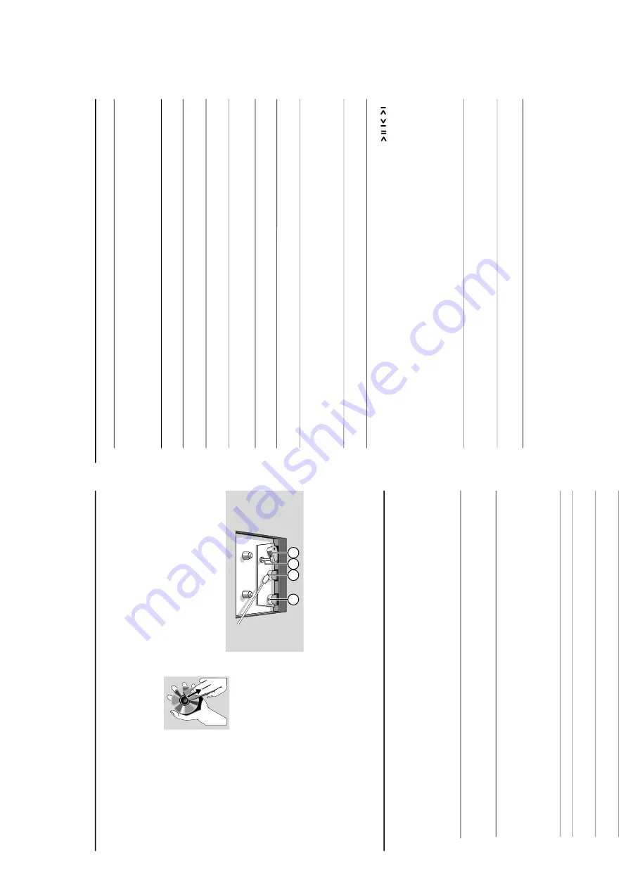
Cleaning Discs
●
When a disc becomes dir
ty
,
clean it with a cleaning cloth.
Wipe the disc from the centre
out.
●
Do not use solv
ents such as
benz
ene
, thinner
, commerciall
y
availab
le cleaner
s,
or antistatic
spr
ay intended for analogue records.
Cleaning the disc lens
●
After prolonged use
, dir
t or dust may
accum
ulate at the disc lens.
To
ensure good
pla
yback quality
, clean the disc lens with Philip
s
CD Lens Cleaner or an
y commercially a
vailab
le
cleaner
. Follo
w the instr
uctions supplied with
cleaner
.
Cleaning the Heads and the
Ta
pe P
aths
●
To
ensure good recording and pla
yback quality
,
clean the heads
A
,the capstan(s)
B
,and
pressure roller(s)
C
after ever
y 50 hour
s of
tape oper
ation.
Caution:
Do not r
otate the heads during
cleaning.
●
Use a cotton swab slightly moistened with
cleaning fluid or alcohol
.
●
Y
ou can also clean the heads by pl
ay
ing a
cleaning tape once
.
A
A
B
C
Demagnetising the heads
●
Use a demagnetising tape a
vailable at y
our
dealer
.
Tr
oub
leshooting
RADIO RECEPTION
Radio r
eception is poor
.
–
If the signal is too weak,
adjust the antenna or
connect an exter
nal antenna f
or better reception.
–
Increase the distance betw
een the Micro HiFi
System and y
our
TV or
VCR.
TAPE OPERA
TION / RECORDING
Recor
ding or pla
yback cannot be made
.
–C
lean deck par
ts,
see
“Maintenance”.
–
Use only nor
mal (IEC I) tape f
or recording.
“
CHECK TAPE
”
is displa
y
ed.
–
Appl
y a piece of adhesive tape
ov
er the missing
tab space
.
The ta
pe deck door cannot open.
–
Remo
ve and reconnect the
AC
po
w
er plug and
switch on the system again.
GENERAL
The system does not r
eact when buttons
–
Remo
ve and reconnect the
AC
po
w
er plug and
ar
e pr
essed.
switch on the system again.
Sound cannot be hear
d or is of poor
–
Adjust the volume
.
quality
.
–D
isconnect the headphones.
–
Check that the speaker
s are connected cor
rectl
y.
–
Check if the str
ipped speaker wire is clamped.
The left and right sound outputs ar
e
–
Check the speaker connections and location.
re
ve
rsed.
The r
e
mote contr
ol does not function
–
Select the source (CD or
TUNER,
for example)
pr
operl
y.
before pressing the function b
utton (
,
,
).
–
Reduce the distance betw
een the remote control
and the system.
–I
nser
t the batter
y with its polar
ities
(+/– signs) aligned as indicated.
–
Replace the
batter
y.
–P
oint the remote control directl
y toward
IR sensor on the front of the system
.
The timer is not w
orking.
–
Set the clock cor
rectl
y.
–
Press
TIMER ON / OFF to switch on the time
r.
–
If a recording is in progress, stop the recording.
The Clock/Timer setting is erased.
–P
ow
er has been inter
rupted or the pow
er cord
has been disconnected.
Reset the clock/time
r.
1-11
Summary of Contents for MC-V320
Page 8: ...PREPARATIONS AND CONTROLS 1 8 2 3 1 8 6 4 5 7 9 0 º ª 27 24 ...
Page 12: ...1 12 TROUBLESHOOTING ...
Page 14: ...2 2 2 2 ...
Page 16: ...4 1 4 1 SET WIRING DIAGRAM ...
Page 18: ...CIRCUIT DIAGRAM FRONT BOARD 5 2 5 2 ...
Page 19: ...LAYOUT DIAGRAM FRONT BOARD COMPONENT SIDE 5 3 5 3 LAYOUT DIAGRAM FRONT BOARD SMD SIDE ...
Page 22: ...6 2 6 2 CIRCUIT DIAGRAM ...
Page 23: ...6 3 6 3 POWER PCB LAYOUT ...
Page 26: ...AM FM TUNER IC TA2149BN AM FM TUNER IC TA2149BN BLOCK DIAGRAM Pins Description 7 2 7 2 ...
Page 27: ...AM FM TUNER IC TA2149BN Pins Description Pins Description AM FM TUNER IC TA2149BN 7 3 7 3 ...
Page 28: ...AM FM TUNER IC TA2149BN Pins Description AM FM TUNER IC TA2149BN Pins Description 7 4 7 4 ...
Page 30: ...DIGITAL TUNING IC TC9257F DIGITAL TUNING IC TC9257F 7 6 7 6 IC BLOCK DIAGRAM ...
Page 31: ...7 7 7 7 DIGITAL TUNING IC TC9257F Pins Description ...
Page 32: ...CIRCUIT DIAGRAM TUNER BOARD NON CENELEC 7 8 7 8 ...
Page 36: ...MICROPROCESSOR TMP87EP26F MICROPROCESSOR TMP87EP26F BLOCK DIAGRAM 8 2 8 2 PINS DESCRIPTION ...
Page 37: ...8 3 8 3 MICROPROCESSOR TMP87EP26F PINS DESCRIPTION POWER DRIVER IC TA2092N ...
Page 40: ...DIGITAL SERVO PROCESSOR TC9462F BLOCK DIAGRAM 8 6 8 6 ...
Page 44: ...MICROPROCESSOR TA2153FN BLOCK DIAGRAM 8 10 8 10 ...
Page 45: ...CIRCUIT DIAGRAM MCU VCD BOARD 8 11 8 11 ...
Page 46: ...LAYOUT DIAGRAM MCU VCD BOARD COMPONENT SIDE 8 12 8 12 ...
Page 47: ...8 13 8 13 LAYOUT DIAGRAM MCU VCD BOARD SMD SIDE ...
Page 50: ...9 2 9 2 CONNECTION PCB CIRCUIT DIAGRAM ...
Page 51: ...9 3 9 3 CONNECTION PCB LAYOUT DIAGRAM ...
Page 56: ...MAIN BOARD CIRCUIT DIAGRAM 10 4 10 4 ...
Page 57: ...10 5 10 5 TAPE PART CIRCUIT DIAGRAM ...
Page 58: ...MAIN PCB COMPONENT LAYOUT 10 6 10 6 ...
Page 59: ...MAIN PCB SMD LAYOUT 10 7 10 7 ...


